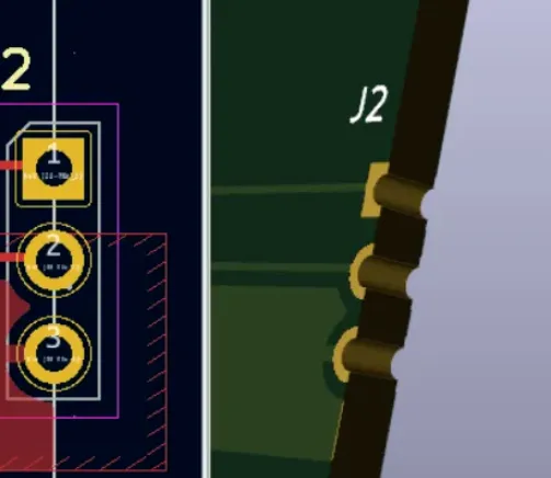
Many hardware engineers finish a schematic in KiCad, run a quick DRC, export Gerbers, and still receive fab house feedback about missing apertures, mismatched drill files, incomplete BOMs, or footprints that fail assembly. The problem is rarely the schematic itself. It is the incomplete view of KiCad as only a pair of editors instead of a connected ecosystem that spans design, verification, libraries, extensions, and manufacturing hand-off.
Understanding the full KiCad ecosystem - its native tools, libraries, community resources, plugins, and manufacturing links - lets you move from open-source design to reliable fabrication and assembly with fewer iterations. This article maps that ecosystem, shows how each piece fits the real engineering workflow (schematic -> PCB -> DRC -> manufacturing outputs -> DFM -> fab/assembly), and explains where manufacturing services such as AIVON close the loop.
What Is Included in the KiCad Ecosystem?
KiCad is more than the Schematic and PCB editors. The ecosystem consists of five practical layers that professionals actually use:
- Design tools - Schematic Editor, PCB Editor, Footprint Editor, Symbol Editor, 3D Viewer, and supporting utilities (DRC, netlist, plotting).
- Libraries - Official and community symbol, footprint, and 3D model collections, plus the ability to create and maintain project-specific libraries.
- Community resources - Official documentation, KiCad forums, GitHub repositories, and shared project examples that provide real board data rather than theory.
- Plugins - Python-based extensions that add BOM tools, design-rule helpers, fabrication exporters, and ordering workflows.
- Manufacturing services - Fabrication and assembly partners that accept KiCad outputs (or direct plugin submissions) and return DFM feedback, quotes, and production boards.
These layers form a continuous path: design decisions made in the editors are constrained by library quality, verified by DRC and plugins, packaged into manufacturing files, and validated by the fab house. Treating any layer in isolation is the most common source of delayed prototypes.
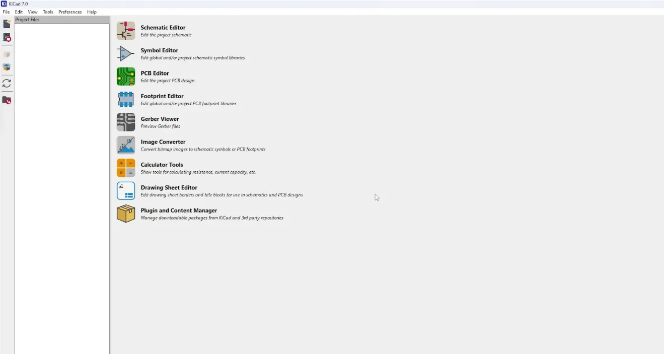
Core KiCad Tools Explained
Schematic Editor
The Schematic Editor captures connectivity, assigns footprints, and generates the netlist that drives the PCB. Engineers need it whenever a new design starts or when a change must propagate cleanly to layout.
Practical workflow: place symbols from verified libraries, set reference designators and values early, run Electrical Rules Check (ERC) before netlist export, and annotate only after the circuit is stable. Common mistakes include using generic symbols without assigned footprints or leaving hierarchical sheets poorly annotated; both produce incomplete netlists and later assembly errors.
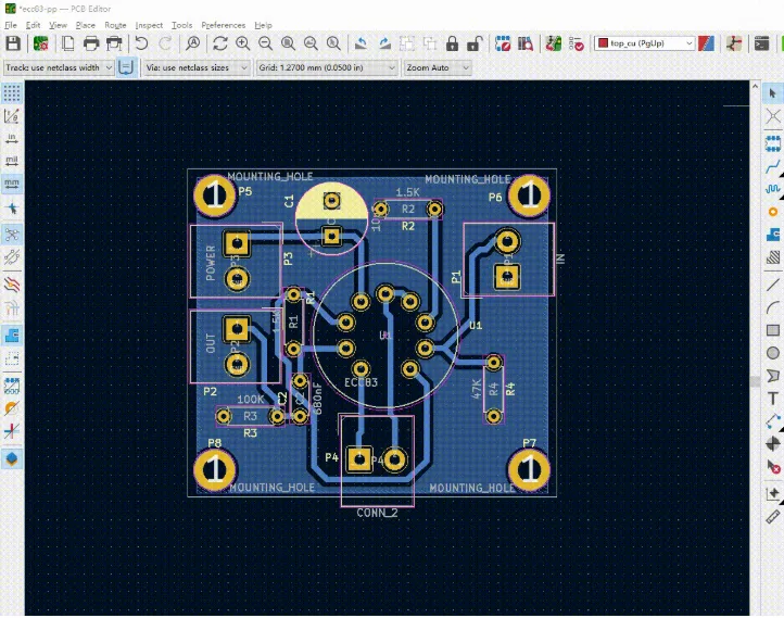
PCB Editor
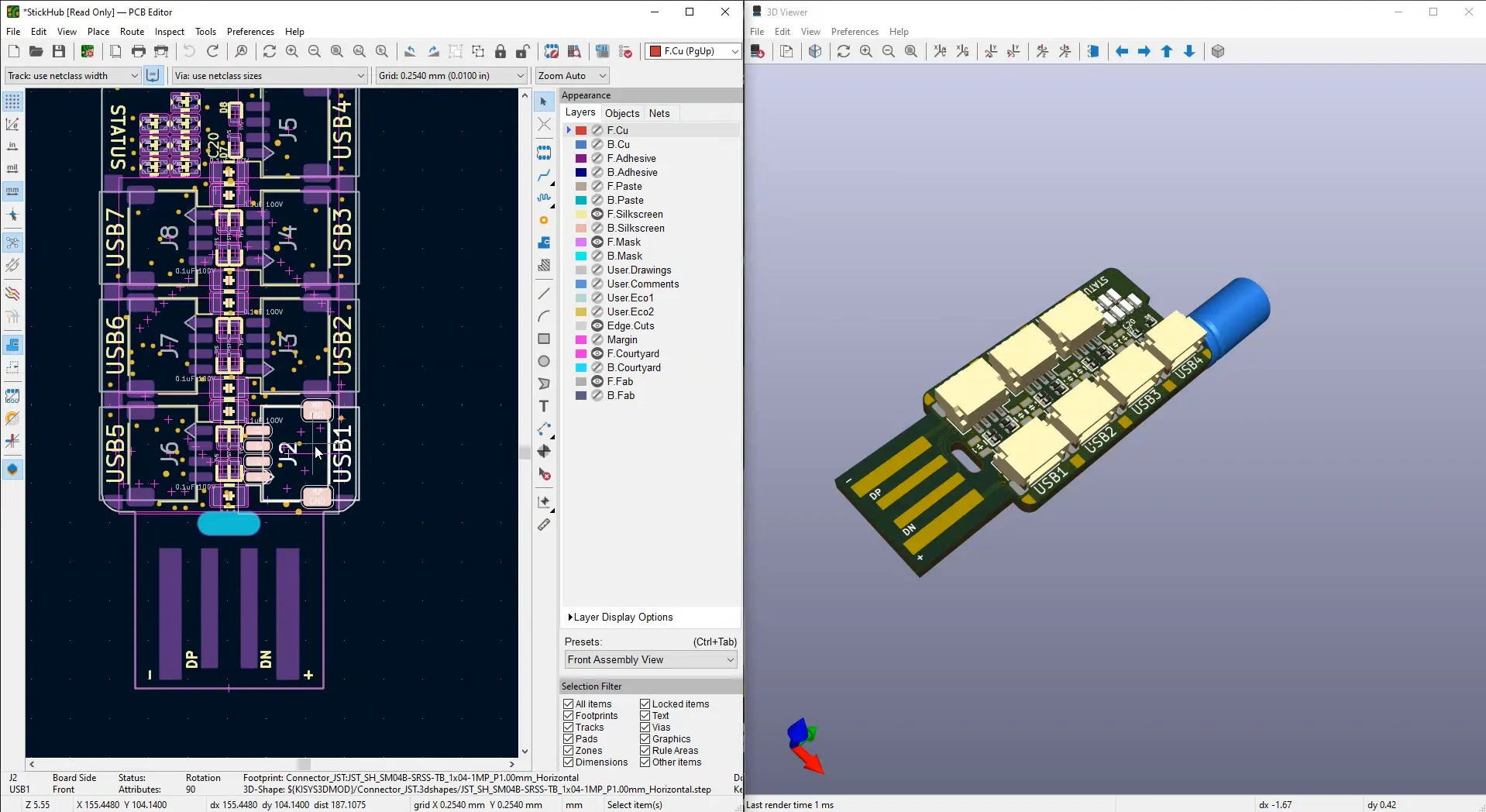
The PCB Editor turns the netlist into copper, silkscreen, solder mask, and mechanical layers. It is the stage where most DFM decisions are locked in: trace width, clearance, via size, copper balance, and stack-up.
Recommended practice: load board setup (layer stack, design rules, net classes) before placing any footprint. Run interactive DRC continuously rather than only at the end. Keep copper pours connected with thermal reliefs appropriate to the fab's process, and verify that all copper is covered by solder mask or defined as exposed pads.
Footprint Editor
The Footprint Editor creates or modifies the physical land patterns that the assembler will place components on. Use it when official libraries lack a part, when a variant package is required, or when a custom mechanical outline is needed.
Best practice: start from an IPC-compliant template, measure the actual component datasheet, add courtyard and fabrication layers, and include 3D model association. Test the footprint on a small test board before committing it to a production library.
3D Viewer
The 3D Viewer renders the board with component models so mechanical collisions, connector clearances, and enclosure fit can be checked before tooling. It becomes essential once the board must fit a housing, stack with another PCB, or clear tall components.
Workflow tip: assign accurate 3D models early and re-check after every major placement change. Many engineers discover keep-out violations or connector interference only in the 3D view.
Useful KiCad Libraries and Resources
Symbol Libraries
Official KiCad libraries plus community contributions supply most common parts. Project-specific or company libraries are added for proprietary or frequently used components. Guidance: prefer symbols that already carry footprint and 3D associations. When creating a new symbol, document the manufacturer part number and any alternate packages in the properties.
Footprint Libraries
Footprint quality directly determines solderability and mechanical reliability. Official libraries follow IPC guidelines for many packages; community footprints vary widely. Best practice: maintain a curated "approved" library. For every new footprint, verify pad geometry against the datasheet and the fab's minimum features.
3D Models
3D models (STEP or WRL) enable mechanical validation and help the assembler. Recommendation: attach the model inside the Footprint Editor so it travels with the footprint. Check scale and origin carefully - incorrect models produce false collision reports.
KiCad Plugins: Extending Design Capabilities
Plugins turn KiCad into a workflow tool rather than a pure drawing package. They fall into two practical groups:
Design plugins help with BOM generation, interactive BOM viewers, design-rule assistants, and length-matching utilities. They reduce manual spreadsheet work and catch errors before Gerber export.
Manufacturing plugins prepare or submit fabrication data. Typical functions include improved Gerber/drill packaging, stack-up visualization, and direct quote or order interfaces.
AIVON's KiCad plugin belongs to the manufacturing group. After the board passes DRC and the manufacturing outputs are ready, the plugin can extract the necessary files and present a quotation path without leaving the KiCad environment. This shortens the usual cycle of exporting a zip, uploading to a website, waiting for manual review, and iterating on feedback.
From Open-Source Design to Professional Manufacturing
The KiCad design flow ends with a set of manufacturing files:
- Gerber (or Gerber X2 / ODB++) for copper, mask, silkscreen, and paste.
- Excellon or equivalent drill files (including plated and non-plated holes).
- BOM with reference, value, footprint, and preferably manufacturer part number.
- Pick-and-place (centroid) file with X/Y, rotation, and side.
- Optional stack-up and fabrication notes.
Manufacturers sit at the far end of the ecosystem. They convert the digital package into physical boards, apply process rules, and often return a DFM report. A good manufacturer also accepts the BOM and centroid for assembly, checks component availability, and flags orientation or polarity issues. The connection works best when the designer has already applied realistic design rules inside KiCad.
How AIVON Extends the KiCad Ecosystem
Once the design tools, libraries, and plugins have produced a clean set of manufacturing files, the remaining gap is reliable quotation, DFM feedback, and production. AIVON fills that gap as a manufacturing service that accepts standard KiCad outputs.
Typical workflow after KiCad design completion:
- Finalize DRC and export Gerbers, drills, BOM, and pick-and-place.
- Use the AIVON plugin or web interface to submit the package.
- Receive a quotation that reflects the actual stack-up, quantity, and options chosen.
- Review any DFM notes returned by the manufacturing team.
- Proceed to fabrication and, if required, assembly.
FAQ
Q1: What files do I need to export from KiCad for PCB manufacturing?
A1: At minimum: Gerber files for every copper, mask, silkscreen, and paste layer; drill files (plated and non-plated); a BOM; and a pick-and-place file. Include a fabrication drawing or notes that define board outline, stack-up, and any special requirements. Always run a final DRC before export.
Q2: How do I keep KiCad libraries consistent across a team?
A2: Maintain a shared, version-controlled library path (Git or similar) that contains only approved symbols, footprints, and 3D models. Point every project to that path and prohibit ad-hoc community footprints on production boards.
Q3: Can KiCad plugins submit boards directly for quotation?
A3: Yes. Manufacturing-oriented plugins, including the AIVON plugin, can package the necessary files and open a quotation workflow without forcing a manual upload. Verify that the plugin matches your KiCad version.
Q4: Why does my board pass KiCad DRC but still receive DFM complaints?
A4: KiCad DRC enforces the rules you set. If those rules are more aggressive than the fabricator's process capability (trace/space, annular ring, soldermask clearance), the CAM review will flag them. Align your board setup with the manufacturer's published capabilities.
Q5: Is KiCad suitable for professional PCB assembly, not just prototypes?
A5: Yes, provided libraries are controlled, design rules match the chosen process, manufacturing files are complete, and a capable assembly partner is used. Many production boards are designed entirely in KiCad and successfully assembled at volume.