Most engineers who open KiCad for the first time already know how to draw a schematic on paper. The real problem appears later: the board that comes back from the fab house has wrong footprints, missing vias, or copper that violates the manufacturer's minimum clearances. The design looked fine on screen, yet the physical PCB fails assembly or fails DRC at the factory.
This KiCad tutorial walks through the complete, production-ready path—from a new project to manufacturing files that a fab can actually build. You will learn the decisions that affect yield, the common mistakes that waste money, and how to move from schematic to Gerbers, drill files, and assembly data without surprises.
KiCad Design Workflow Overview
A professional PCB flow in KiCad is not a series of isolated screens. It is a continuous chain:
KiCad Design → Design Rule Check (DRC) → Generate Manufacturing Files → Gerber Export → Drill File Generation → BOM / Pick-and-Place Export → DFM Review → PCB Manufacturing → PCB Assembly
Each stage feeds the next. A footprint error discovered only at the pick-and-place stage is expensive. Catching it during schematic annotation or footprint assignment costs almost nothing.
The four practical stages engineers use every day are:
- Schematic capture – define the circuit and assign real parts
- Component selection – choose footprints that match the manufacturer's library or your own validated set
- PCB layout – place, route, and pour copper while respecting real fabrication limits
- Manufacturing output – produce clean Gerbers, Excellon drills, BOM, and centroid files
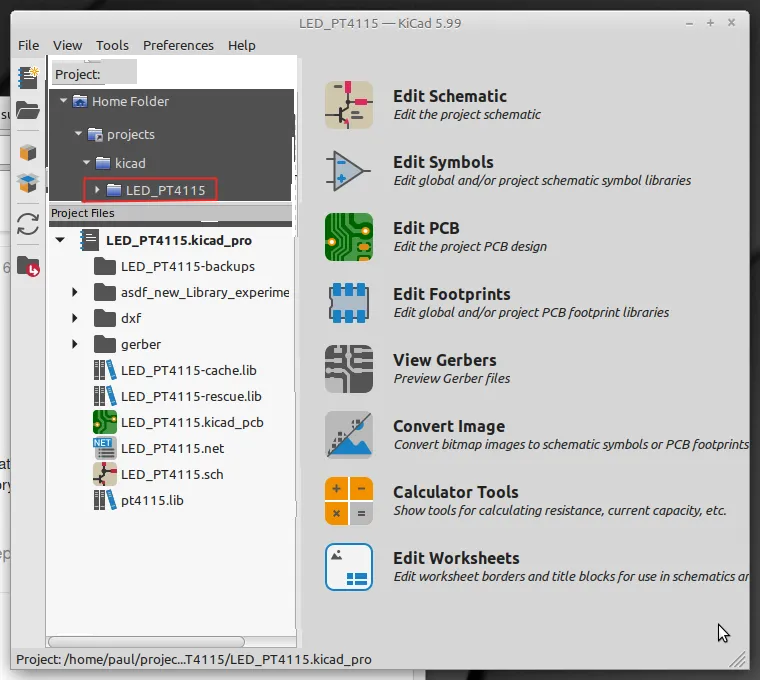
Step 1: Create a New KiCad Project
Open KiCad and create a new project. The project folder becomes the single source of truth. It contains the schematic (.kicad_sch), board (.kicad_pcb), and later the manufacturing outputs.
Recommended structure:
- Keep the project name short and free of spaces (use underscores).
- Store the project on a local drive or version-controlled folder; network paths can break relative library links.
- Immediately set the project-specific library tables if you use company or vendor libraries.
Basic settings worth checking before drawing anything:
- Page size and title block (important for documentation handed to manufacturing).
- Default net class (you will refine clearance and track width later).
- Units (mm is standard for most fab houses).
A clean project structure prevents the classic "missing library" error that appears only when someone else opens the files months later.
Step 2: Design Your Circuit Schematic
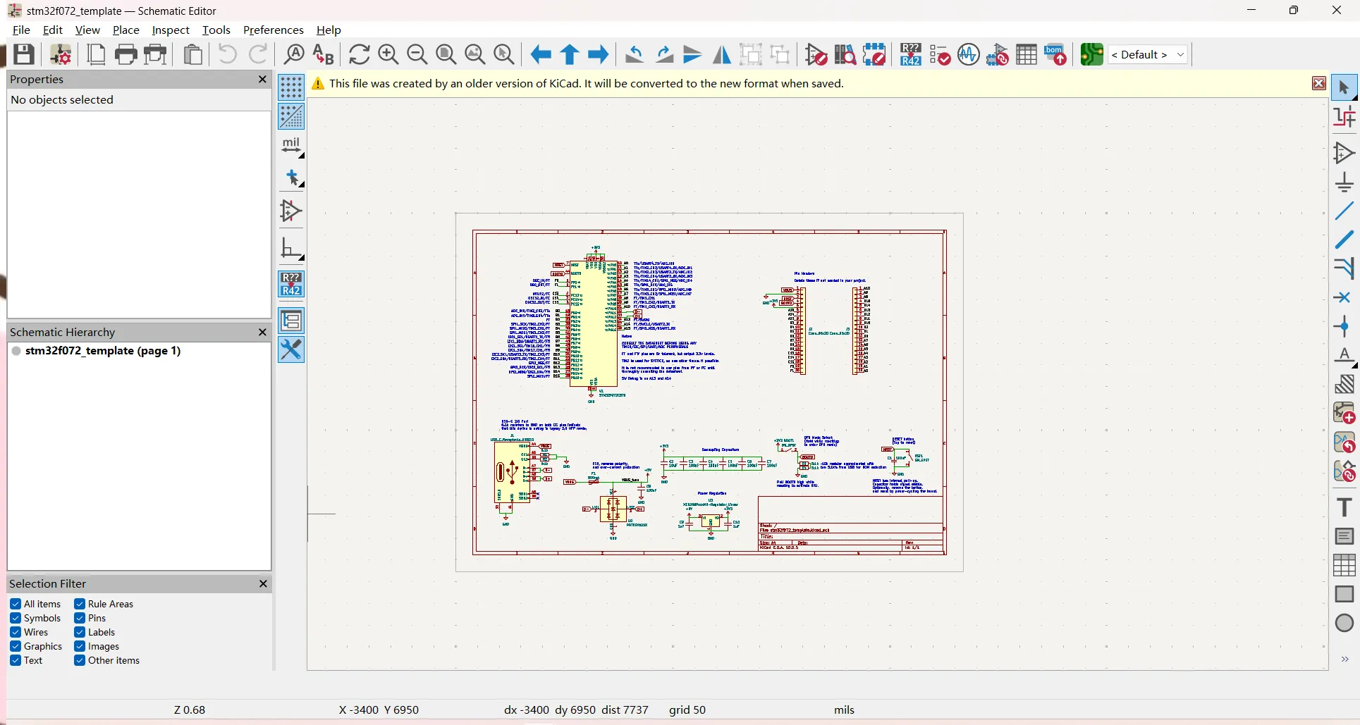
Schematic capture is where electrical correctness is established. Bad net names or missing power flags create silent failures that only appear after the board is fabricated.
Practical workflow:
- Place symbols from the official or your validated libraries. Prefer symbols that already have a footprint association.
- Wire the nets. Use hierarchical sheets for anything beyond a few dozen components—flat schematics become unreadable and error-prone.
- Assign reference designators systematically (U for ICs, R for resistors, C for capacitors, etc.).
- Run the Electrical Rules Check (ERC). Fix every error and most warnings. Power-flag and pin-type mismatches are the most common real-world issues.
Manufacturing perspective: the schematic drives the BOM. An incorrect value or missing manufacturer part number at this stage forces a respin or costly last-minute substitutions. Professional teams lock the BOM early and treat schematic changes after layout as controlled engineering changes.
Common beginner mistake: placing a symbol without verifying its footprint association. The board will later show the wrong pad pattern even though the schematic looks perfect.
Step 3: Create PCB Layout in KiCad
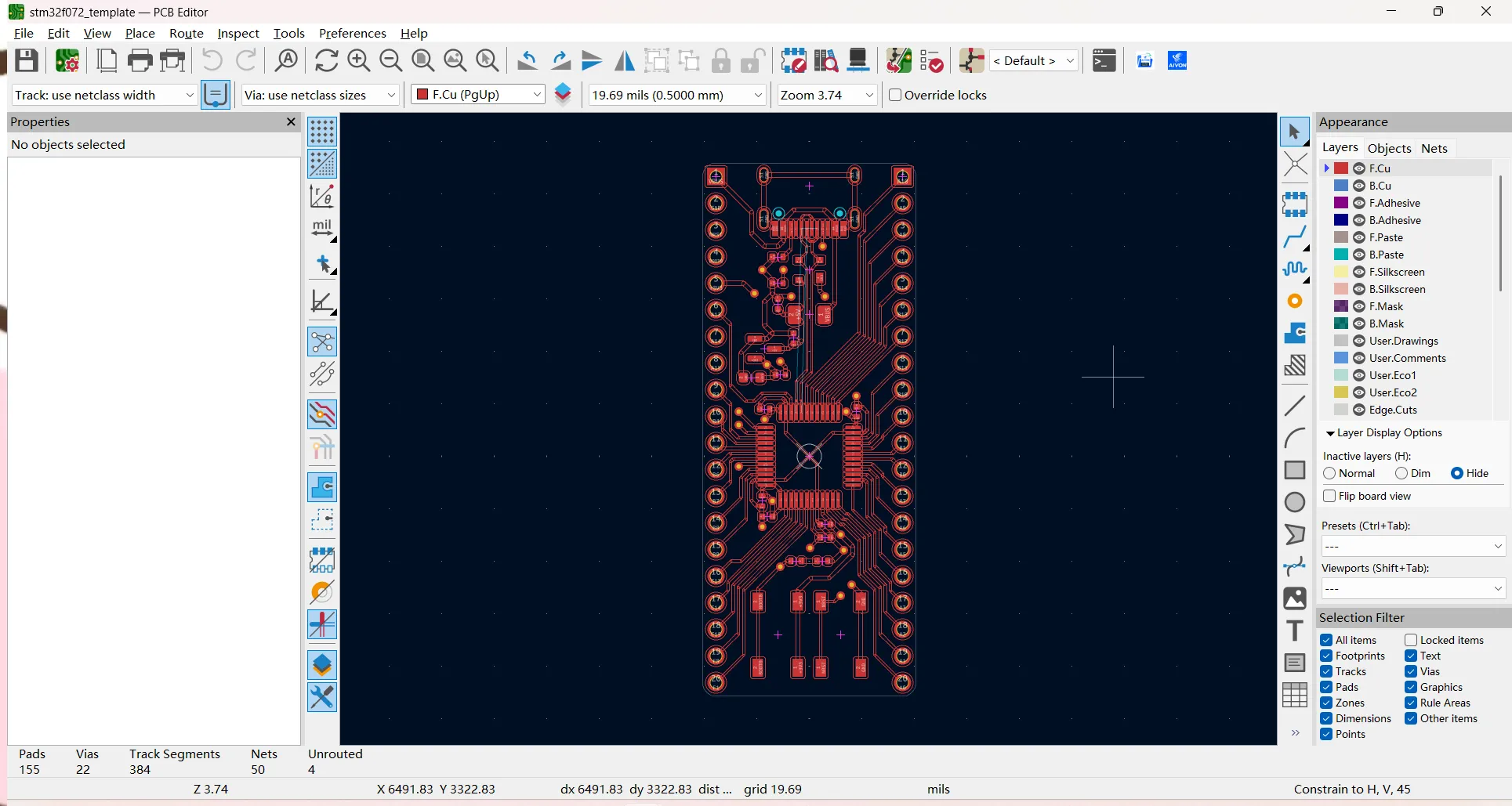
After the schematic is clean, switch to the PCB Editor and update the board from the schematic. This imports the footprints and netlist.
Assign Footprints
Double-check every footprint against the actual component datasheet and the manufacturer's recommended land pattern. Prefer footprints that already include the correct courtyard, silkscreen, and solder-mask openings.
Component Placement
Place critical components first: connectors, crystals, power regulators, and high-speed ICs. Keep analog and digital sections separated when possible. Leave enough space for the fab's minimum keep-out around board edges and mounting holes.
Routing
Start with power and ground. Use the Interactive Router with the correct net class rules. For signals that matter (clocks, differential pairs, high-current paths), set length matching or impedance targets early. Avoid 90-degree corners on high-speed nets; 45-degree or arc routes reduce reflections.
Copper Zones
Create continuous ground and power planes. Use thermal reliefs for through-hole pads unless the current is high enough to justify solid connections. Run the zone fill and then the DRC—unconnected zones are a frequent source of manufacturing failures.
Manufacturing perspective: clearance and track width must match the fab's process capability, not just the default KiCad values. A 0.1 mm clearance that passes local DRC may still be rejected by a low-cost manufacturer whose minimum is 0.15 mm. Always set design rules to the actual fab constraints before final routing.
Step 4: Prepare KiCad Files for Manufacturing
Never send a board to fabrication without a clean DRC and complete manufacturing package.
- Design Rule Check
Run DRC with the rules set to the target manufacturer's capabilities. Fix every error. Warnings about silkscreen overlapping pads or copper too close to the board edge should also be resolved. - Generate Gerber Files
Use Plot → Gerber. Select the layers your fab actually needs (usually F.Cu, B.Cu, F.SilkS, B.SilkS, F.Mask, B.Mask, Edge.Cuts, and any internal layers). Enable "Use Protel filename extensions" only if the manufacturer requests it; otherwise use the modern KiCad naming. - Drill Files
Generate Excellon drill files (both plated and non-plated if required). Include the drill map for visual verification. - Additional Manufacturing Files
BOM (CSV or Excel) with manufacturer part numbers, Pick-and-place (centroid) file, Optional: 3D STEP model for mechanical review.
A complete package lets the manufacturer run their own DFM check without asking you for missing layers or drill data.
Step 5: Send KiCad Design to PCB Manufacturer
Two practical paths exist.
Manual upload workflow
Zip the Gerbers, drill files, and BOM. Upload to the manufacturer's portal, fill in board parameters (thickness, copper weight, surface finish, quantity), and wait for a DFM review. This method works with any fab but requires careful file naming and manual parameter entry.
AIVON plugin workflow
After the manufacturing files are generated, engineers can use the AIVON KiCad plugin to upload the design directly, obtain an instant quotation, and place the order for PCB fabrication and assembly. The plugin reduces the chance of missing layers or incorrect stack-up parameters because the data is taken straight from the KiCad project.
In both cases the goal is identical: give the PCB manufacturer a clean, complete data package so their DFM tools can confirm the board is manufacturable before production starts.
Common Beginner Mistakes in KiCad PCB Design
- Wrong footprints – The schematic symbol is correct, but the pad pattern does not match the real component. Result: parts cannot be soldered. Always verify the footprint against the datasheet land pattern.
- Missing drill information – Forgetting to generate or include the Excellon file. The fab receives copper layers but no hole locations.
- Incorrect design rules – Using KiCad's default 0.2 mm clearance when the chosen manufacturer requires 0.15 mm minimum or when high-voltage isolation demands larger gaps. Always load the fab's design-rule set before final DRC.
- Silkscreen over pads or vias – Looks minor on screen but causes soldering defects or inspection failures.
- Unfilled copper zones – Ground plane appears continuous in the 3D view but is actually fragmented, creating return-path problems.
These mistakes are almost always caught by a proper DRC plus a quick visual check of the Gerber set in a free Gerber viewer before ordering.
FAQ
Q1: How do I export Gerber files correctly in KiCad for manufacturing?
A1: Open the PCB Editor, go to File → Plot, select Gerber format, choose the required layers (copper, silkscreen, solder mask, board outline), set the output directory, and plot. Then generate the Excellon drill files from the same dialog. Always open the resulting files in a Gerber viewer to confirm nothing is missing.
Q2: What is the difference between ERC and DRC in KiCad?
A2: ERC (Electrical Rules Check) runs on the schematic and catches unconnected pins, power conflicts, and pin-type mismatches. DRC (Design Rule Check) runs on the PCB and checks clearances, track widths, via sizes, and other physical constraints. Both must be clean before manufacturing.
Q3: Can I use KiCad for professional PCB manufacturing and assembly?
A3: Yes. Many commercial products are designed entirely in KiCad. The critical steps are correct footprints, manufacturer-matched design rules, complete Gerber/drill/BOM packages, and a final DFM review by the fabricator. Tools such as the AIVON plugin further streamline the ordering process.
Q4: Why does my KiCad board fail at the PCB manufacturer even though DRC passed?
A4: Local DRC only checks the rules you set. If those rules are looser than the manufacturer's process limits, or if you omitted layers or drill files, the fab's own DFM check will reject the job. Always configure design rules to the actual fab capabilities and include every required manufacturing file.
Q5: How do I assign the correct footprints in a KiCad schematic?
A5: Select the symbol, open its properties, and set the Footprint field to a verified library entry. Prefer footprints that include courtyard, silkscreen, and solder-mask layers matching the component datasheet. After assignment, update the PCB from the schematic and visually inspect each footprint.
Following this workflow turns KiCad from a drawing tool into a reliable path from idea to manufactured board. Start with a clean project, keep the schematic and footprints synchronized, respect real fabrication limits, and always deliver a complete manufacturing package. The boards that come back will match what you designed.