Finishing a PCB layout in KiCad is only half the job. The real friction begins when you must turn that design into manufacturing files, package them correctly, upload them to a fabricator, wait for a quote, and hope nothing was missed. Manual Gerber export, drill file generation, BOM cleanup, and pick-and-place preparation consume time and introduce errors that only surface after the boards arrive.
The AIVON KiCad Plugin removes most of that friction. It acts as a direct bridge between the KiCad PCB Editor and AIVON's fabrication and assembly platform, so engineers can move from a completed, DRC-clean board to a production-ready order without leaving their design environment.
This article explains what the plugin is, why it matters for professional KiCad workflows, the prerequisites, practical usage, and how it fits into the complete path from schematic to assembled boards.
What Is the AIVON KiCad Plugin?
The AIVON KiCad Plugin is a fabrication-oriented action plugin that connects a finished KiCad board directly to AIVON's online quoting and ordering system.
It automates the generation and packaging of the manufacturing data set that fabricators require:
- Gerber files (copper, soldermask, silkscreen, paste, Edge.Cuts)
- Excellon drill files
- Bill of Materials (BOM)
- Pick-and-place (centroid) files
Instead of manually plotting layers, checking output in GerbView, zipping files, and uploading them through a browser, the plugin handles the export steps and transfers the package to AIVON. The engineer then reviews the quote, selects options (quantity, surface finish, solder mask color, assembly if needed), and places the order.
How it simplifies the PCB ordering workflow
Traditional path:
KiCad design → DRC → manual Plot Gerbers → Drill files → BOM export → PnP export → zip → upload → quote form → order
With the plugin:
KiCad design → DRC → launch AIVON plugin → review auto-generated package → quote and order
Key benefits for KiCad users
- Reduced file-preparation errors (missing layers, incorrect units, incomplete BOMs)
- Faster iteration for prototypes
- Consistent manufacturing data format preferred by AIVON's engineering review team
- Direct access to AIVON's capabilities (24-hour prototypes, multilayer, HDI, flex/rigid-flex, Rogers, full PCBA with component sourcing)
- One less context switch between design tool and manufacturer portal
The plugin does not replace good design practice. It simply eliminates the repetitive, error-prone hand-off steps that sit between a clean DRC and a physical board.
Prerequisites Before Installation
Before installing the plugin, prepare the following:
Required KiCad version
The plugin targets current stable KiCad releases that support the Plugin and Content Manager (PCM) and action plugins (KiCad 6 and newer; verify the exact minimum version listed in the plugin package or AIVON documentation). Always run the latest stable release for best compatibility with external plugins.
AIVON account preparation
Create a free account at aivon.com. New users typically receive welcome credits that can be applied to the first PCB or PCBA order. Having an account ready allows the plugin to authenticate and transfer files without interruption.
Board readiness checklist
- Schematic fully annotated and footprints assigned
- PCB layout complete
- Design Rule Check (DRC) run with zero critical violations
- Board outline closed on Edge.Cuts
- Netlist updated from schematic
Skipping DRC or leaving open outline segments will still cause manufacturing problems even if the plugin packages the files correctly.
How to Install the AIVON KiCad Plugin
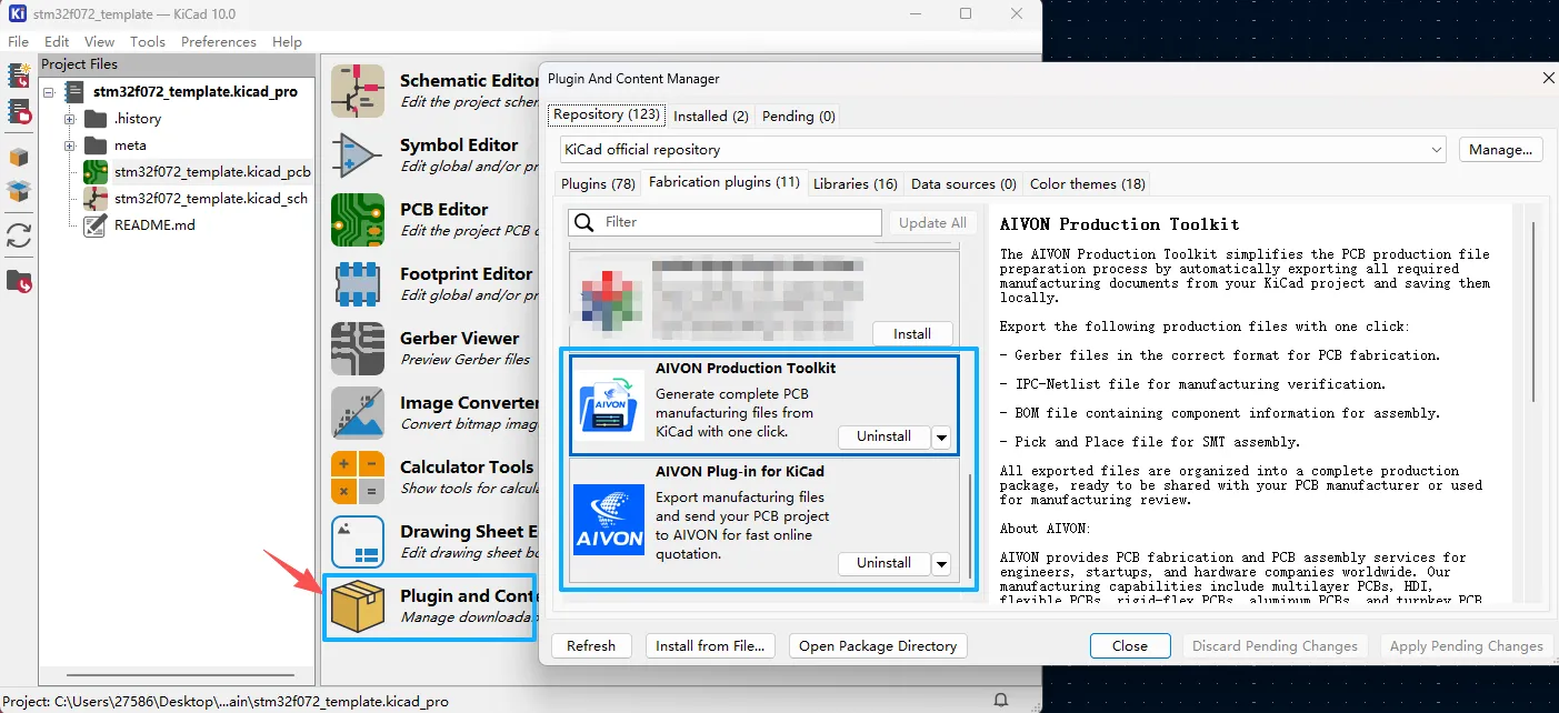
Most manufacturer plugins install through KiCad's built-in Plugin and Content Manager:
- Open KiCad (main project manager window).
- Go to Tools → Plugin and Content Manager.
- Search for "AIVON" or the exact plugin name provided by AIVON.
- Click Install, then Apply Pending Changes.
- Restart the PCB Editor if the plugin icon does not appear immediately.
If the plugin is distributed as a zip file (common for newer or manufacturer-specific packages):
- Download the official zip from AIVON's site or documentation.
- In Plugin and Content Manager, choose Install from File… and select the zip.
- Apply changes and restart.
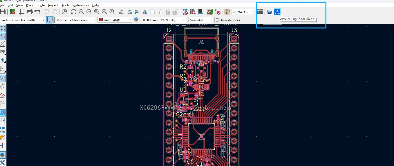
After installation the AIVON plugin appears under Tools → External Plugins or as a toolbar icon inside the PCB Editor.
Using the Plugin to Order PCBs from KiCad
Recommended workflow once the board is ready:
- Open the project in the PCB Editor.
- Run DRC one final time and resolve any remaining issues.
- Launch the AIVON KiCad Plugin.
- The plugin generates the manufacturing package (Gerbers, drills, BOM, PnP). Review the generated file list if the interface shows it.
- The plugin opens or redirects to the AIVON quote page with the files already uploaded.
- Confirm or adjust parameters: quantity, layers (auto-detected in most cases), board thickness, copper weight, surface finish, solder mask and silkscreen colors, and whether assembly is required.
- For PCBA orders, ensure the BOM contains manufacturer part numbers and the PnP file uses millimetre coordinates with correct rotation.
- Review the instant or engineer-reviewed quote, apply any available credits, and place the order.
AIVON's process includes an engineering file review. This catches common issues (insufficient clearances, non-standard stack-ups, missing polarity marks) before production starts, reducing the chance of scrap or delayed delivery.
Integrating the Plugin into the Complete KiCad-to-Manufacturing Workflow
Professional PCB work follows a continuous chain:
KiCad Design
Schematic capture → footprint assignment → layout and routing → copper zones and stack-up definition.
Design Rule Check (DRC)
Validate clearances, track widths, via sizes, and manufacturing constraints against the rules you set for the intended process (prototype vs production).
Generate Manufacturing Files
The AIVON plugin (or manual Plot) produces Gerbers, drills, BOM, and PnP.
Gerber Export & Drill File Generation
Correct layer selection, Protel-style extensions, millimetre units, and a drill map are essential. The plugin standardises these settings for AIVON.
BOM / Pick-and-Place Export
Accurate designators, manufacturer part numbers, and rotation values prevent assembly errors.
DFM Review
AIVON engineers check the package. Early feedback on min trace/space, annular rings, or impedance requirements can be fed back into KiCad design rules for the next revision.
PCB Manufacturing
Fabrication of the bare board (24-hour options available for standard FR-4 prototypes).
PCB Assembly
If ordered, component sourcing and SMT/through-hole assembly follow, using the same BOM and PnP data.
The plugin shortens the middle of this chain. It does not eliminate the need for good DRC settings or clear stack-up notes, but it removes the manual packaging steps that often introduce the most avoidable defects.
Best Practices and Common Pitfalls
Best practices
- Always run a full DRC with your target manufacturer's minimum capabilities loaded as custom rules before launching the plugin.
- Keep the board outline on Edge.Cuts only and ensure it is a single closed shape.
- For assembly, use AIVON's preferred BOM template columns and confirm polarity marks are clear on the silkscreen or assembly drawing.
- Include a short README or fabrication notes (stack-up, controlled impedance, special materials) when the design is non-standard.
- After receiving boards, compare the physical result against the original Gerbers in GerbView to close the feedback loop.
Common mistakes that still cause problems
- Launching the plugin on a board that still has DRC violations.
- Incomplete footprint assignment or missing manufacturer part numbers in the BOM.
- Using mil units or mixed units in drill files.
- Forgetting to update the board from the schematic before export, so designators or footprints are out of date.
- Ordering advanced features (HDI, rigid-flex, heavy copper) without first confirming capability and lead time with AIVON.
These issues are manufacturing risks, not plugin failures. The plugin makes the hand-off cleaner; design quality remains the engineer's responsibility.
AIVON provides both PCB fabrication and PCBA services, allowing the workflow to extend from prototype PCB production toward assembled boards when a project requires it.
For users placing their first order with AIVON, the Welcome Credits program provides up to $60 in new-user support, including a $30 manufacturing credit and up to $30 in shipping support. The new customer offer is designed to make it easier for engineers and makers to move from a completed PCB design to their first physical prototype.
FAQ
Q1: Does the AIVON KiCad Plugin replace manual Gerber export?
A1: For most standard orders it can. The plugin generates the required Gerber, drill, BOM, and pick-and-place files and transfers them to AIVON. Complex designs may still benefit from a manual review in GerbView before ordering.
Q2: What KiCad version do I need for the AIVON plugin?
A2: Current stable releases that support the Plugin and Content Manager (typically KiCad 6 and later). Always check the plugin's own documentation or AIVON support for the exact supported versions.
Q3: Can I order PCB assembly (PCBA) through the plugin?
A3: Yes. After the board files are transferred you can add assembly options, upload or confirm the BOM and pick-and-place data, and receive a combined quote that includes component sourcing and SMT.
Q4: What happens if my design has DFM issues?
A4: AIVON performs an engineering review on uploaded files. You will receive feedback on problems such as insufficient clearances, non-manufacturable vias, or missing polarity marks before production begins, giving you a chance to correct the KiCad design.
Q5: Is an AIVON account required to use the plugin?
A5: Yes. An account is needed for authentication, quoting, and order placement. New accounts usually receive welcome credits that lower the cost of the first prototype.