Selecting the Correct Trace Width in KiCad
Selecting the correct trace width is one of the most common decisions that directly determines whether a board works reliably or fails under load, heat, or manufacturing variation. Too narrow a trace on a power net can overheat and lift copper. Too wide a high-speed signal can destroy impedance matching and create reflections. In KiCad, the decision is not only about drawing a line—it becomes a design-rule constraint that flows all the way through DRC, Gerber generation, and fabrication.
This article shows how to set practical trace-width rules in KiCad, how to relate those rules to current capacity, signal integrity, and real PCB manufacturing limits, and how professional engineers balance the three so the finished board survives both electrical stress and the fab process.
Why Trace Width Selection Matters
Trace width controls two fundamental limits: how much current the copper can carry without excessive temperature rise, and how the trace interacts with the surrounding dielectric for signal integrity.
When current is higher than the trace can handle, the copper heats up. Temperature rise accelerates oxidation, increases resistance further, and in extreme cases causes the trace to delaminate or open. On the signal side, width (together with copper thickness, dielectric height, and dielectric constant) sets the characteristic impedance. A mismatch creates reflections that degrade timing margins or raise bit-error rates.
These electrical decisions also become manufacturing constraints. Fabricators have minimum and preferred track widths; violating them lowers yield and raises cost. Engineers who treat width as a pure electrical choice often discover the problem only after the first prototype returns with open circuits or high resistance on power rails.
Understanding PCB Trace Width Basics
Relationship Between Width and Current
Current-carrying capacity of a PCB trace is governed primarily by cross-sectional area (width × copper thickness) and the allowed temperature rise above ambient. Thicker copper or wider traces carry more current for the same temperature rise. Industry practice commonly uses IPC-2221 or IPC-2152 charts (or online calculators based on them) to arrive at a starting width.
A practical rule of thumb used by many engineers for 1 oz copper and 10 °C rise is roughly:
- 10 mil (0.25 mm) ≈ 0.5–1 A
- 20–25 mil ≈ 1.5–2 A
- 50 mil ≈ 3–4 A
These numbers change significantly with copper weight, internal versus external layer, and whether the board has good thermal vias or copper pours nearby. Always treat calculator results as a starting point and then apply a safety margin for continuous load and ambient temperature.
Signal vs Power Traces
Power traces are sized for current and voltage drop. Signal traces are sized for impedance and routing density. Mixing the two without net classes is a frequent source of DRC errors and later manufacturing surprises.
In most designs the majority of nets are low-current digital or analog signals that can safely use the fabrication minimum or a slightly larger preferred width (e.g., 6–8 mil). Power nets (VCC, GND returns that carry significant current, motor drivers, LED strings) require dedicated wider classes. High-speed differential pairs usually sit in their own class with tightly controlled width and gap.
Setting Trace Width Rules in KiCad
KiCad enforces width through Net Classes and Design Rules rather than forcing the designer to remember a number for every track.
Creating Net Classes
- Open Board Setup → Design Rules → Net Classes.
- Create classes that match the electrical needs of the board, for example:
- Default (signals)
- Power_1A
- Power_3A
- Power_5A
- Diff_50ohm or Diff_90ohm
- For each class set Track Width, Via Size, and Clearance.
- Optionally define a minimum and preferred track width; the router and interactive router will respect the preferred value while DRC still checks the absolute minimum.
Assigning Different Width Rules
Assign nets to classes in one of three ways:
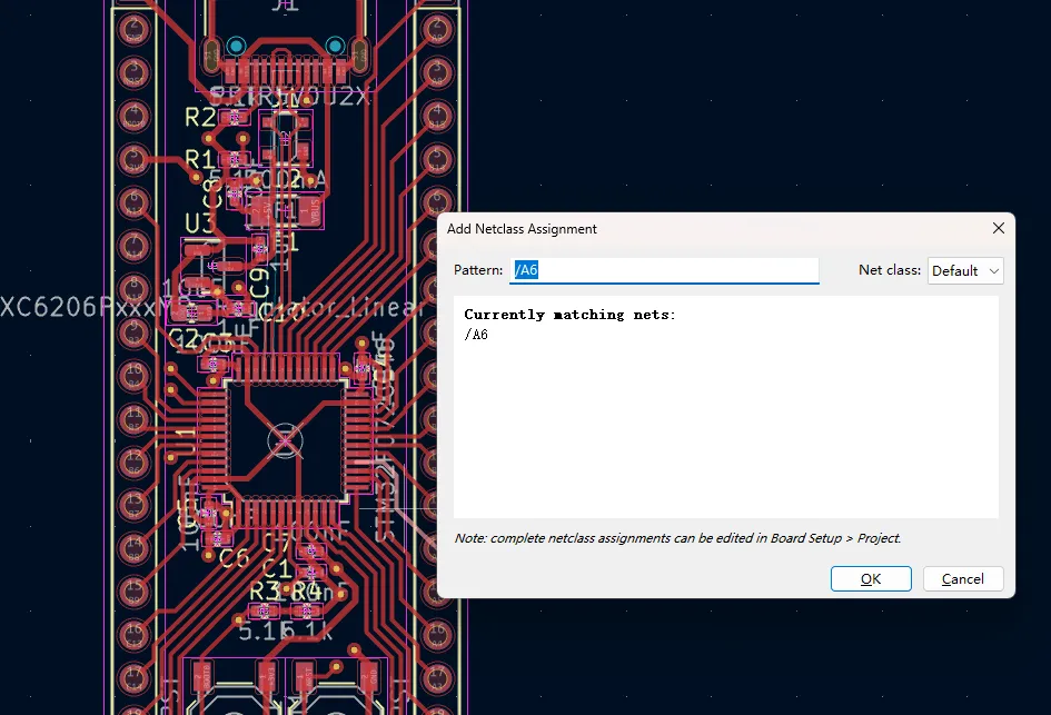
- By net name pattern in the Net Classes panel (e.g., /VCC* → Power_3A).
- Manually in the schematic or PCB by selecting the net and changing its class.
- Through hierarchical sheet or bus naming conventions that make pattern matching reliable.
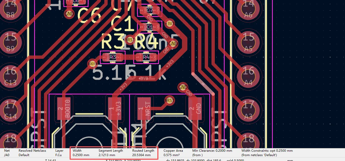
Once classes exist, the interactive router automatically uses the class width. Running DRC after placement will flag any track that is narrower than its class minimum or any clearance violation. This is the point where design intent becomes enforceable before Gerber generation.
Factors Affecting Trace Width Selection
Copper Thickness
Most prototype and low-volume boards use 1 oz (35 µm) outer copper. 2 oz copper roughly doubles current capacity for the same width and temperature rise, but it also changes etch tolerances and minimum feature size. When the board house quotes 2 oz, update the KiCad copper thickness in Board Setup → Physical Stackup so that impedance calculators and DRC remain consistent.
Current Requirements
Measure or estimate continuous current, not just peak. Add margin for ambient temperature above 25 °C and for nearby heat sources. For return paths that share copper with many signals, calculate the total return current rather than treating each power pin independently.
Temperature Rise
A 10 °C rise is conservative for most commercial products. A 20–30 °C rise is sometimes accepted on power planes or heavy copper when the application allows higher surface temperature. Document the chosen rise so that later revisions or different copper weights can be recalculated consistently.
Layer Location
External layers dissipate heat better than internal layers because they have air or solder mask on one side. The same current on an internal layer usually needs a wider trace. In multilayer boards, engineers often keep high-current nets on outer layers or stitch them with thermal vias to copper pours on adjacent layers.
Trace Width Guidelines for Different Applications
Low-Current Signals
Digital GPIO, I²C, SPI, UART, and most analog sensor nets typically use 6–10 mil (0.15–0.25 mm). This width is well within the capability of almost every modern fab and keeps routing density high. Only increase width when the net must travel long distances and voltage drop or noise susceptibility becomes an issue.
Power Circuits
Create dedicated net classes. Example starting points for 1 oz external copper and ~10–15 °C rise:
| Continuous Current | Suggested Track Width | Notes |
|---|---|---|
| ≤ 0.5 A | 8–12 mil | Can often stay in Default class |
| 1 A | 20–25 mil | Power_1A class |
| 2–3 A | 40–50 mil | Power_3A class; consider copper pour |
| > 5 A | Copper pour + vias | Trace alone is rarely sufficient |
Always verify with a calculator that includes your exact copper weight and layer.
High-Speed Signals
Width is dictated by target impedance, not by current. For a 50 Ω single-ended microstrip on a typical 1.6 mm FR-4 stack-up with 1 oz copper, width is often in the 8–12 mil range depending on dielectric height. Differential pairs (USB, HDMI, Ethernet, PCIe) use a specific width-and-gap combination. In KiCad, place these nets in a dedicated class and use the length-tuning and differential-pair tools so that both members stay at the design width.
Manufacturing Limits and PCB Fabrication Considerations
Every fabricator publishes a minimum trace width and minimum spacing that they can reliably etch. Common prototype capabilities today are 4–6 mil (0.1–0.15 mm) for standard processes; tighter features require advanced processes and higher cost. Using the absolute minimum on every net lowers yield because of under-etch or over-etch variation.
Professional practice is to set the KiCad minimum track width a little above the fabricator's absolute minimum (for example, 6 mil when the fab advertises 5 mil) and to use the preferred width for most routing. This improves yield without sacrificing density.
After layout is complete the normal workflow is:
- Run full DRC (including net-class width and clearance checks).
- Generate Gerbers and drill files.
- Visually inspect the Gerber layers for unexpectedly narrow tracks or acute angles that the etcher may attack.
- Submit the package for fabrication.
When the design is ready for production, engineers export the manufacturing files and can submit them directly for quotation and fabrication. Services such as AIVON accept standard Gerber sets generated from KiCad and provide DFM feedback on minimum feature sizes, copper balance, and panelization before the boards are made. This closes the loop between the net-class rules you defined in KiCad and the physical process that will etch those traces.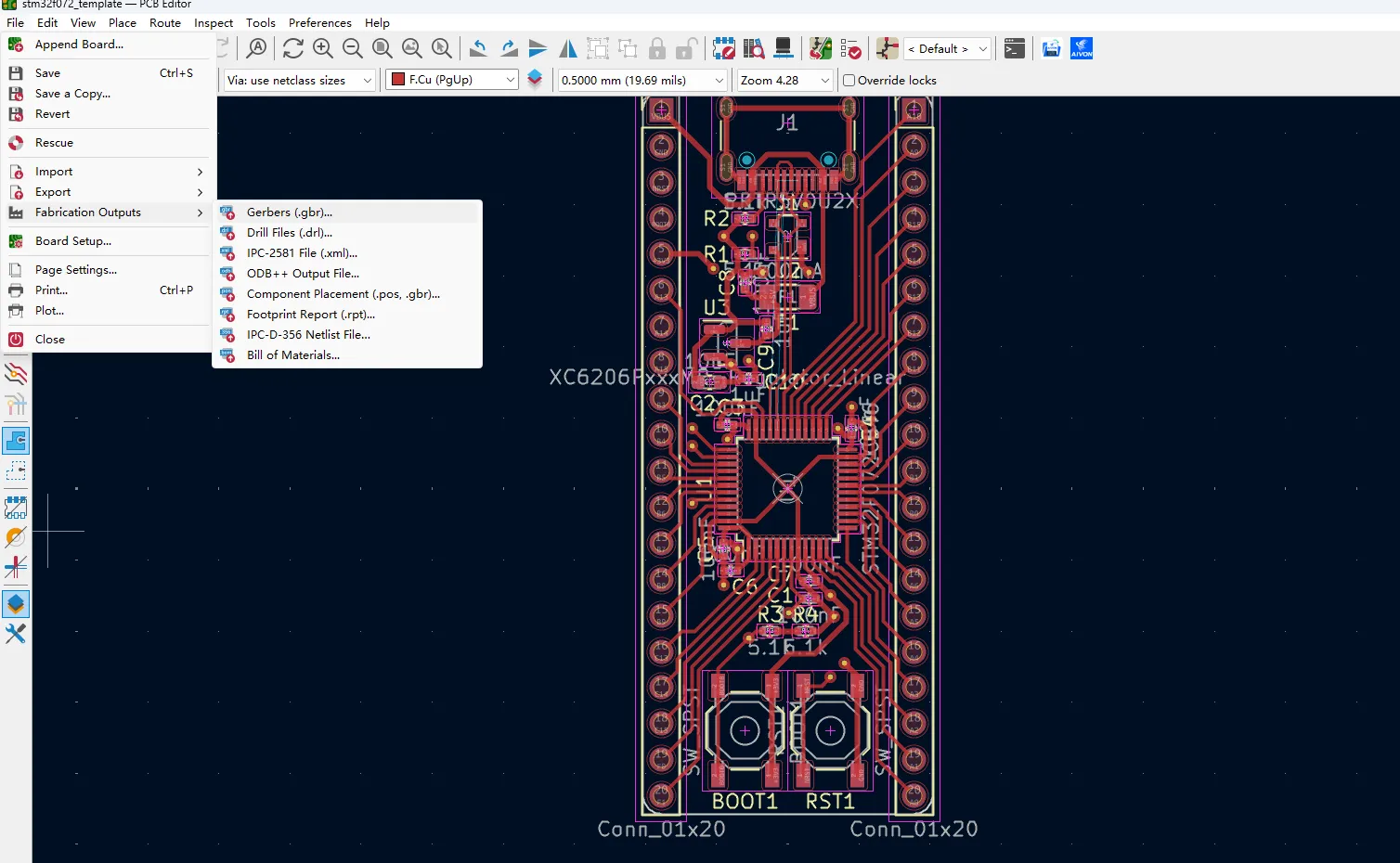
FAQ
Q1: How do I calculate the correct PCB trace width for a given current in KiCad?
A1: Use an external IPC-based calculator with your copper weight, allowed temperature rise, and whether the trace is internal or external. Enter the resulting width into the appropriate Net Class in Board Setup. KiCad itself does not calculate current capacity; it only enforces the width you assign.
Q2: What is the minimum trace width I should use in KiCad for standard PCB fabrication?
A2: Check the capabilities of your chosen fabricator. For most prototype services a safe design minimum is 6 mil (0.15 mm). Set this value as the absolute minimum in the Net Class or in Custom Rules, and use a slightly larger preferred width for everyday routing to improve yield.
Q3: Can I use different trace widths on the same net in KiCad?
A3: Yes, but only if you intentionally allow it. The interactive router follows the net-class width. You can manually change a segment's width afterward; DRC will still flag any segment that falls below the class minimum. For controlled-impedance nets it is better to keep the entire net at the design width.
Q4: How does copper thickness affect the trace width I should choose?
A4: Doubling copper thickness (1 oz → 2 oz) roughly doubles the current capacity for the same width and temperature rise. Update the stack-up copper weight in KiCad so that any impedance calculations remain accurate, and adjust the Net Class widths accordingly.
Q5: Should high-speed signals use the same width rules as power traces?
A5: No. High-speed signals are sized for impedance control, not for current. Create a separate net class with the exact width and clearance required by the stack-up and the target impedance. Power nets use wider classes sized for thermal and voltage-drop limits.