










KiCad Hub
KiCad Hub: Guides, Tips, and Best Practices
Featured Blog

What Is KiCad? A Complete Introduction to Open Source PCB Design Software
Learn what KiCad is, its core features for schematic design, PCB layout, 3D visualization, and manufacturing output. Discover why engineers choose this free open-source tool and how to move from design to professional PCB fabrication.

Latest Blogs
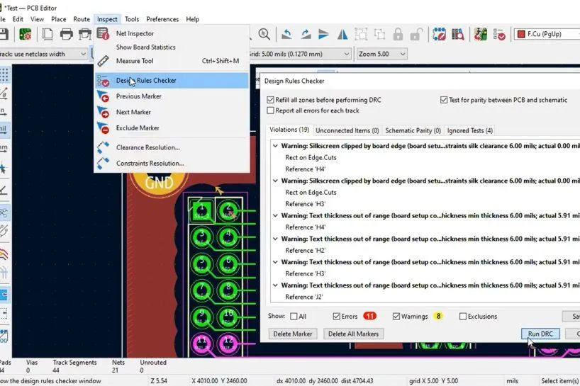
KiCad Manufacturing Checklist: 10 Things to Check Before Ordering PCB
Use this KiCad manufacturing checklist to verify layer count, dimensions, copper, drills, footprints, DRC, Gerbers and assembly files before ordering. Avoid DFM rejects and ensure your board is production-ready.
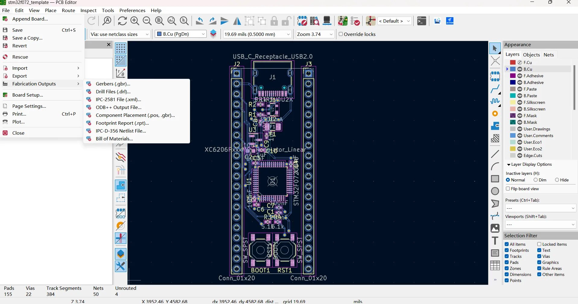
How to Prepare KiCad Files for PCB Assembly: Gerber, BOM and Pick-and-Place Guide
Learn how to prepare KiCad files for PCB assembly. This guide covers Gerber generation, BOM with manufacturer part numbers, pick-and-place files, common mistakes and essential checks to ensure smooth fabrication and assembly.
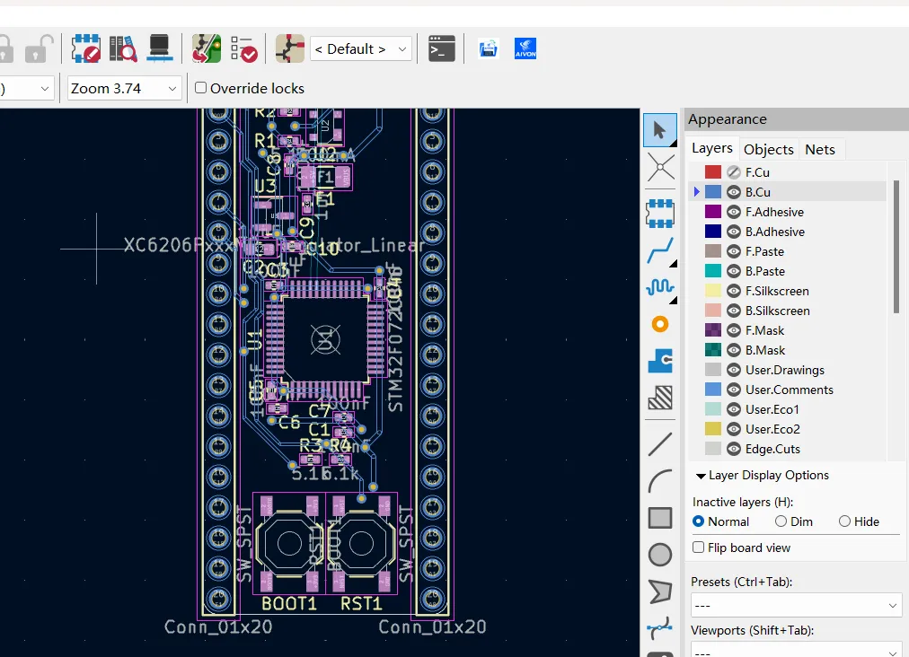
Designing PCB Stackups in KiCad for Manufacturing: Layer Planning Guide
Learn how to design PCB stackups in KiCad for manufacturing. This guide covers layer structure, 2/4-layer configurations, high-speed considerations, copper thickness and material selection to meet performance and fabrication requirements.
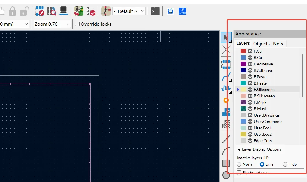
KiCad File Formats Explained: PCB, Schematic, Libraries and Gerber
Learn KiCad file formats including .kicad_pro, schematic, PCB, symbol and footprint libraries, Gerber, drill, BOM and pick-and-place files. Understand which files to send to PCB manufacturers.
KiCad vs Altium vs Eagle: Which PCB Design Software Should You Choose?
Compare KiCad, Altium Designer, and Eagle for PCB design. See costs, features, target users, beginner recommendations, and manufacturing tips to choose the right EDA tool for your projects.

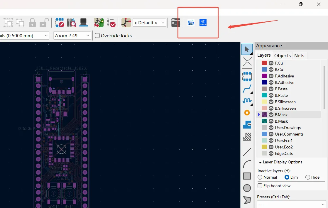
Design PCB in KiCad and Order PCBs Directly with AIVON
AIVON’s official KiCad plugin transfers design data directly to its ordering platform. Skip manual Gerber exports and uploads. Get quotes and order PCBs faster from the PCB Editor.
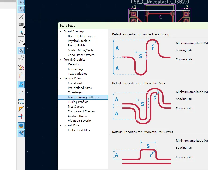
Differential Pair Routing in KiCad: Setup, Rules and Best Practices
Master differential pair routing in KiCad. Learn rule setup, impedance control, length matching, and high-speed best practices for USB, HDMI & Ethernet—plus manufacturing tips that prevent signal integrity failures.
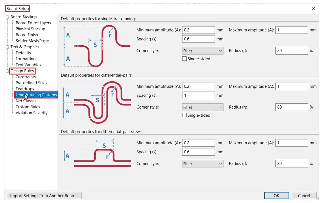
How to Design a PCB Layout in KiCad: Complete Guide for Beginners
Learn how to design a PCB layout in KiCad step by step. This beginner guide covers board setup, design rules, component placement, routing, DRC checks and manufacturing tips to create reliable, production-ready boards.
PCB Component Placement Best Practices in KiCad
Learn proven PCB component placement best practices in KiCad. Improve signal integrity, thermal performance, and manufacturability with functional grouping, high-speed guidelines, and DFM-ready tips.
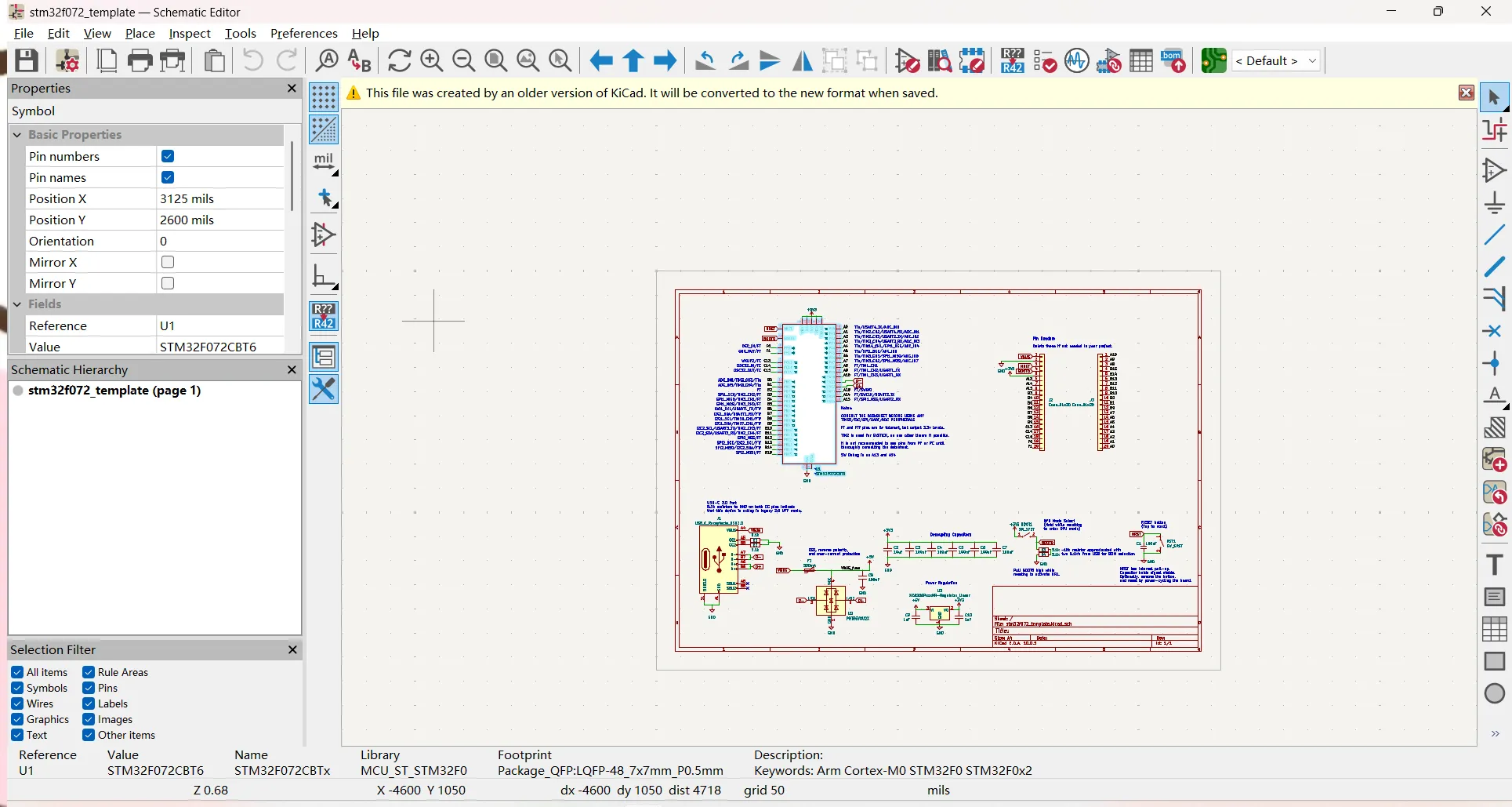
10 PCB Design Tips Every KiCad User Should Know
Master 10 practical PCB design tips for KiCad users. Learn schematic organization, correct footprints, design rules, placement, routing, power/ground design, DRC checks and manufacturing file preparation to boost quality and reduce production issues.
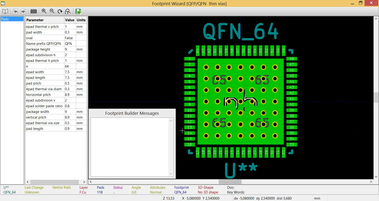
KiCad Footprints Explained: Create, Edit and Manage PCB Footprints
Learn how to create, edit and manage KiCad footprints correctly. This guide covers symbol vs footprint links, library selection, custom pad and courtyard design, plus verification steps that prevent manufacturing and assembly failures.
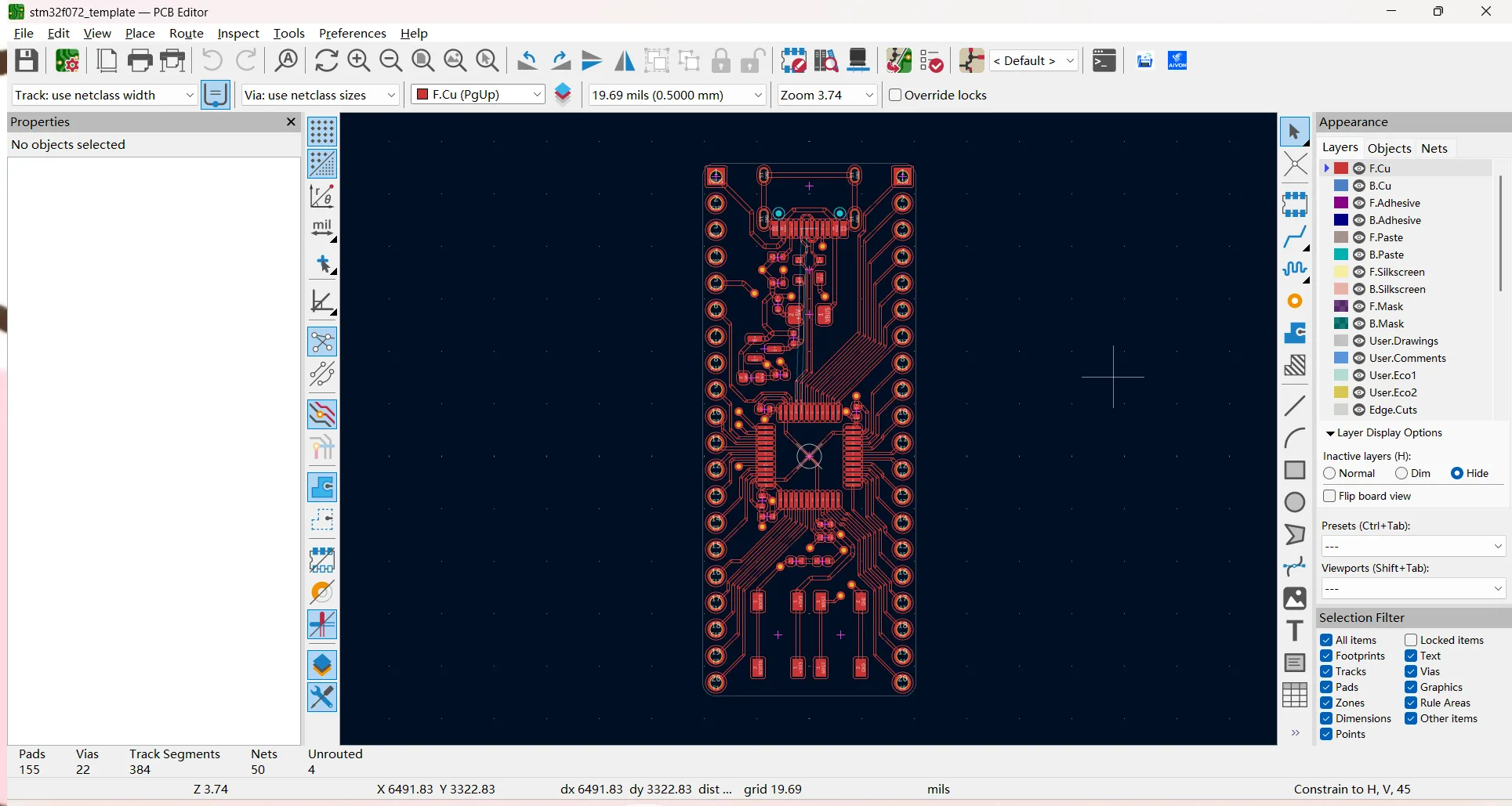
KiCad Tutorial: From Schematic Design to PCB Manufacturing
Learn the complete KiCad workflow from schematic capture and PCB layout to DRC, Gerber export, and manufacturing files. This practical tutorial helps engineers avoid common mistakes and prepare production-ready boards for fabrication and assembly.


