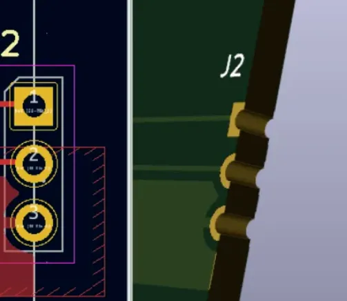
Most PCB failures that reach the factory floor did not begin on the production line. They started weeks earlier in the layout editor—wrong footprints, incomplete manufacturing files, ignored design rules, or components the fab and assembler simply cannot handle. These issues cause holds, respins, extra costs, and delayed projects.
This article examines the most common manufacturing problems KiCad users encounter, explains why they happen from a factory perspective, and gives practical fixes you can apply before generating Gerbers. The goal is to improve design for manufacturability (DFM) so your boards move cleanly from KiCad to fabrication and assembly.
Problem 1: Incorrect Footprint Selection
Causes
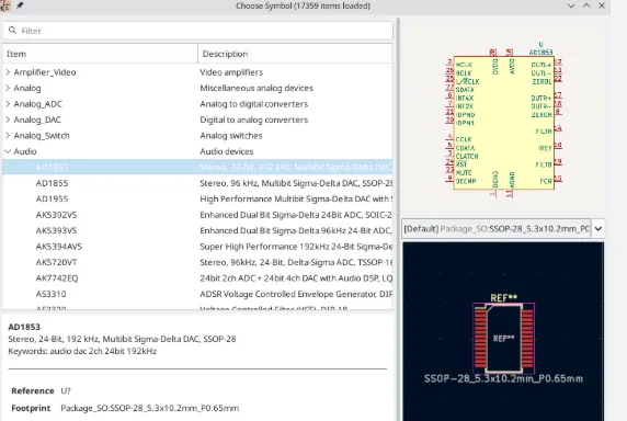
Footprints are often taken from community libraries or auto-assigned without verification against the actual component datasheet. Common mistakes include:
- Pad sizes or shapes that do not match the recommended land pattern
- Incorrect pin 1 orientation or polarity marking
- Missing or malformed courtyards
- Through-hole pads with zero or incorrect drill diameters
- Using a "hand-soldering" variant when the part will be machine-placed
Manufacturing Impact
Incorrect footprints lead to parts that do not sit properly on the pads, poor solder joints, tombstoning, or open connections after reflow. In severe cases the board must be scrapped or extensively reworked. Assembly houses also flag polarity errors that force manual inspection of every board.
Prevention Methods
- Always open the datasheet land-pattern recommendation and compare it to the KiCad footprint in the Footprint Editor.
- Run the footprint against KiCad Library Convention (KLC) checkers when possible.
- Verify pin 1 and polarity markers visually on both the silkscreen and fabrication layers.
- Confirm drill sizes for through-hole parts and set the correct fabrication attributes (SMD vs through-hole).
- After assignment, update the board from the schematic and re-run DRC so courtyard and pad clearances are checked.
From a manufacturing viewpoint, the footprint is the first physical interface between your design and the real component. A few minutes of verification here prevents the most expensive class of assembly failures.
Problem 2: Missing or Incorrect Manufacturing Files
Gerber Issues
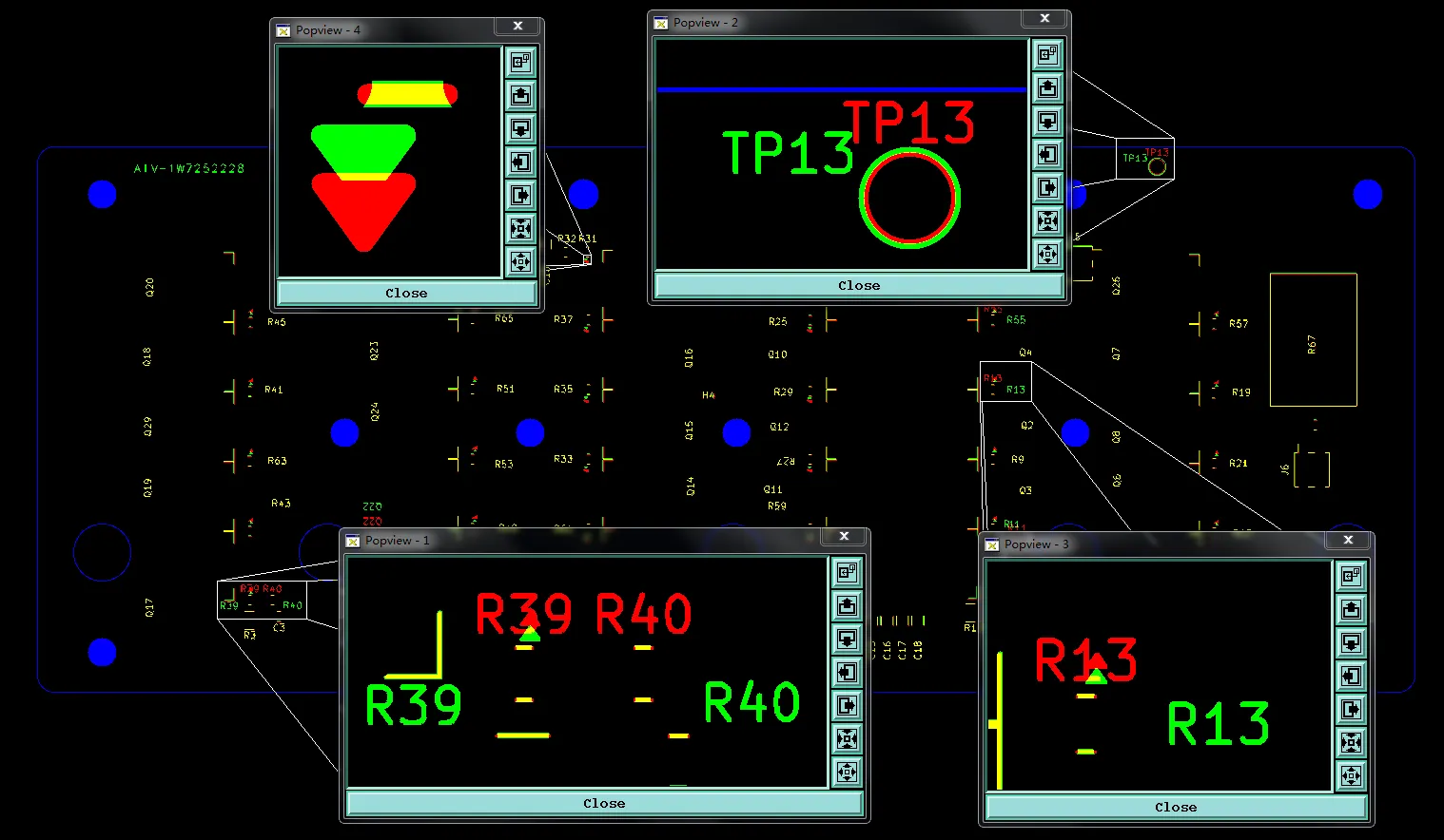
Typical problems include unfilled copper zones (empty power planes), missing board outline (Edge.Cuts not plotted or not closed), silkscreen overlapping pads, or layers plotted with the wrong polarity or aperture settings. Outdated zone fills are especially common—designers change pours but forget to refill before plotting.
Drill File Problems
Drill files are generated separately from Gerbers. Frequent errors are mismatched origins (holes appear shifted relative to pads), mixed units (inches vs millimeters), missing NPTH holes, or submitting a drill map instead of the actual Excellon file. Oval slots rendered as round holes also appear regularly.
Layer Confusion
Copper layers, solder-mask, paste, and mechanical layers are sometimes swapped or omitted. Multi-layer boards may have inner-layer stackup information that does not match the submitted Gerbers, causing impedance or isolation problems.
Prevention Methods
- Always refill all zones (press B) immediately before plotting.
- Use a consistent drill/place file origin for both Gerber and drill exports.
- Plot every required layer and verify the complete set in GerbView or an external viewer.
- Generate drill files in millimeters, Excellon format, with both PTH and NPTH included (or clearly separated if required).
- Name files clearly and package only the manufacturing outputs—never the native .kicad_pcb file.
Manufacturers cannot guess missing data. Incomplete or misaligned files stop production until the designer supplies corrected outputs, adding days of delay.
Problem 3: PCB Design Rule Violations
Clearance Errors
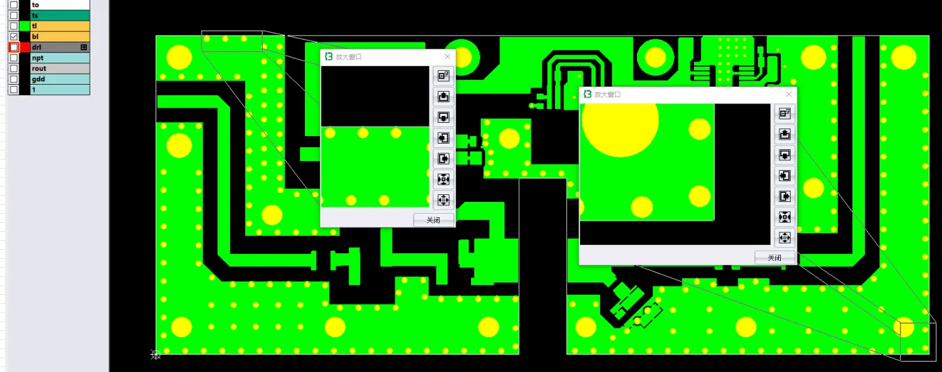
Copper-to-copper, copper-to-hole, or copper-to-board- clearances below the fabricator's minimum create shorts, acid traps, or etching failures. Via-to-via or pad-to-via spacing that is too tight can also cause drill breakage.
Trace Width Issues
Traces narrower than the process capability (or power traces that are under-sized for current) lead to open circuits after etching or excessive heating in operation. Annular rings that are too small around vias or through-holes are another frequent DRC failure that results in breakout.
Unconnected Nets
Ratsnest lines that remain after routing mean nets are electrically incomplete. These are often overlooked when designers rely only on visual inspection.
Prevention Methods
- Configure Board Setup → Design Rules with the actual capabilities of your target manufacturer (minimum track, clearance, annular ring, hole size).
- Run a full Design Rule Check (Inspect → Design Rules Checker) and resolve every error before generating manufacturing files. Treat warnings seriously as well.
- Use custom rules for high-current nets, differential pairs, or high-voltage clearances.
- After any major change, re-run DRC and confirm zero unconnected items.
Design rules are not arbitrary software limits—they mirror the physical constraints of etching, drilling, and plating processes. Violating them turns a theoretically correct schematic into an unmanufacturable board.
Problem 4: Components Cannot Be Manufactured or Assembled
Package Availability
Fine-pitch BGAs, 0201 or smaller passives, or unusual packages may exceed the fabricator's or assembler's standard process windows. Some parts simply have long lead times or have been discontinued.
Assembly Limitations
Height restrictions, polarity marks that are ambiguous or missing, components placed too close for pick-and-place nozzles, or parts that require selective soldering can all stop an assembly line. DNP (Do Not Populate) components left in the pick-and-place file also create confusion.
Prevention Methods
- Check the manufacturer's capability list for minimum pitch, minimum component size, and maximum board thickness/height before finalizing the BOM.
- Ensure every polarized part has a clear silkscreen or fabrication-layer marker.
- Use courtyard clearances that allow the assembler enough space for the nozzle and inspection.
- Mark true DNP parts correctly so they are excluded from both the BOM and position files.
- Prefer commonly stocked packages whenever design constraints allow.
From the factory side, an "unassemblable" component forces either a redesign, a manual process, or a complete board respin. Early communication with the assembler about unusual packages prevents most of these surprises.
How AIVON Engineering Helps KiCad Users Avoid Manufacturing Problems
Even careful designers benefit from a second set of experienced eyes. After you complete the KiCad design, run DRC, and generate Gerbers, drill files, BOM, and pick-and-place data, the next critical step is a professional DFM review.
AIVON's engineering team examines the submitted files for the exact classes of problems described above—footprint and pad issues, missing or misaligned manufacturing layers, clearance and annular-ring violations, stackup and impedance concerns, and assembly feasibility. Feedback is provided before production begins so corrections can be made while changes are still inexpensive.
The review covers both fabrication and assembly readiness. When issues are found, clear recommendations are given (for example, adjusting trace widths for controlled impedance, adding copper pours for reference planes, or clarifying polarity marks). Production support continues through the build so any remaining questions are resolved quickly.
KiCad users can also take advantage of AIVON's workflow tools that simplify packaging and quotation of the design files, reducing the chance of missing layers or mismatched origins during submission. The combination of disciplined design practices in KiCad and professional engineering review before the boards are made dramatically improves first-pass success.
By addressing footprint accuracy, manufacturing-file integrity, design-rule compliance, and component feasibility inside KiCad—and by using professional engineering review—you move from reactive fixes to proactive manufacturable designs. The result is fewer holds, higher first-pass yield, and boards that arrive ready to work.
FAQ
Q1: What is the single most common reason KiCad boards are delayed at the fab house?
A1: Incomplete or incorrectly generated manufacturing files—especially missing board outlines, unfilled copper zones, or drill files that do not share the same origin as the Gerbers. Always verify the full set in a Gerber viewer before uploading.
Q2: How do I set KiCad design rules to match a specific manufacturer?
A2: Open Board Setup → Design Rules → Constraints and enter the minimum track width, clearance, annular ring, and hole size published by the fabricator. Then run a full DRC. Many manufacturers publish KiCad-compatible rule sets or capability tables that can be entered directly.
Q3: Why do my footprints look correct in KiCad but fail at assembly?
A3: The library footprint may not match the actual component's recommended land pattern, or the courtyard and polarity markings may be insufficient. Always cross-check the datasheet land pattern and confirm pin-1 orientation on both the silkscreen and fabrication layers.
Q4: Should I fix every DRC warning or only the errors?
A4: Treat errors as mandatory. Warnings often indicate near-limit conditions (thin annular rings, tight clearances, silkscreen near pads) that still cause manufacturing yield loss. Resolve or consciously waive them with documentation.
Q5: When is the best time to involve a manufacturer's engineering team?
A5: After the board passes internal DRC and the manufacturing files have been generated and visually checked, but before placing a production order. Early DFM feedback catches issues while the design is still easy to change and prevents costly respins.