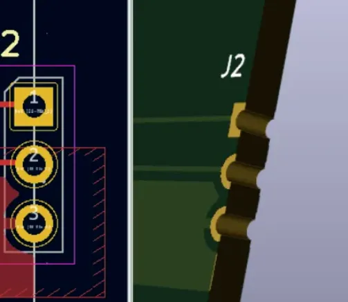
A finished PCB layout in KiCad is not yet ready for production. Fabrication houses do not open native .kicad_pcb files. They require a standardized set of Gerber and drill files that describe every copper feature, solder mask opening, silkscreen marking, board outline, and hole. Incorrect or incomplete files are the single most common reason boards are held, delayed, or fabricated with errors.
This guide walks through the complete, practical process of exporting manufacturing-ready Gerber and drill files from KiCad. You will learn which layers are required, how to configure the export dialogs correctly, how to verify the output, and how to avoid the mistakes that cause the majority of factory rejects. The final sections also show how modern workflows can reduce the manual steps between design and manufacturing.
Why Gerber Files Are Required for PCB Fabrication
Gerber files are the industry-standard vector format that describes each physical layer of the board as a set of apertures and coordinates. They contain no electrical intelligence—only geometry. The fabricator's CAM system uses these files to generate photo-tools, laser plots, and drilling programs.
KiCad converts the internal board database into Gerber data through the Plot function. The quality of that conversion depends entirely on the settings you choose and the state of the design at the moment of export. A missing layer, an unfilled copper zone, or a mismatched origin between Gerbers and drills will produce boards that do not match your intention.
What Manufacturing Files Are Needed from KiCad?
A complete manufacturing package normally includes:
- Gerber files for every copper layer (F.Cu, B.Cu, and any inner layers)
- Solder mask layers (F.Mask, B.Mask)
- Silkscreen layers (F.Silkscreen, B.Silkscreen)
- Solder paste layers (F.Paste, B.Paste) if a stencil is required
- Board outline (Edge.Cuts)
- Drill files in Excellon format (plated and non-plated holes)
- Optional but useful: drill map, fabrication notes, and stack-up documentation
Missing any of these items forces the manufacturer to request clarification or to make assumptions that can lead to errors.
Step 1: Prepare Your KiCad PCB Design Before Exporting
Before opening the Plot dialog, complete these checks:
- Finish all routing and copper pours.
- Run a full Design Rule Check (Inspect → Design Rules Checker) and clear every error.
- Confirm the board outline on the Edge.Cuts layer is a single closed shape.
- Refill all zones (press B or Edit → Fill All Zones). Outdated zone fills are one of the most frequent causes of empty power planes in Gerbers.
- Verify that the drill/place file origin is set (Place → Drill/Place File Origin) and matches the location you intend to use for both Gerbers and drills.
- Check Board Setup → Layers to ensure the correct number of copper layers is defined.
Skipping these steps is the root cause of most "empty layer" and "misaligned drill" problems reported by factories.
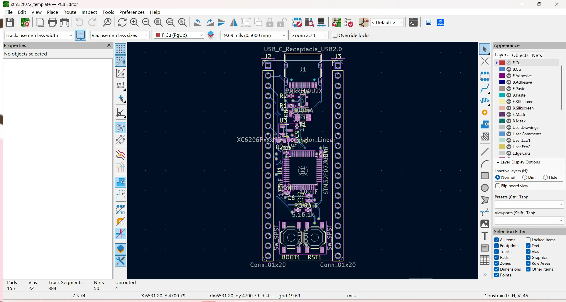
Step 2: Generate Gerber Files in KiCad
- Open the finished board in the PCB Editor.
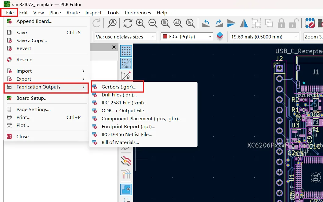
- Go to File → Fabrication Outputs → Gerbers… (or click the Plot icon on the toolbar).
- In the Plot dialog:
- Set the output directory.
- Select every required layer: all copper layers, F.Mask, B.Mask, F.Silkscreen, B.Silkscreen, F.Paste, B.Paste, and Edge.Cuts.
- Enable "Use Protel filename extensions" for maximum compatibility with manufacturers.
- Choose "Gerber" as the plot format.
- Set coordinate format and units consistently (millimeters preferred by most modern fabs).
- Enable "Subtract soldermask from silkscreen" if you want silkscreen automatically clipped away from pads.
- Click Plot to generate the files.
- Review the Output Messages window for any warnings.
The result is a set of individual .gbr (or .gtl, .gbl, etc.) files, one per layer.
Step 3: Generate Drill Files in KiCad
Drill data is exported separately:
- Still in the PCB Editor, go to File → Fabrication Outputs → Drill Files….
- Configure the settings:
- Output directory (same folder as the Gerbers is convenient).
- Drill file format: Excellon.
- Units: Millimeters.
- Zeroes format and precision matching your manufacturer's preference (most accept the KiCad defaults).
- Enable "Use drill/place file origin" so coordinates align with the Gerbers.
- Include both plated (PTH) and non-plated (NPTH) holes, either in one file or separate files according to the fab's requirements.
- Click Generate Drill File.
The output is typically a .drl file (and optionally a drill map). Always generate the drill file after the Gerbers so the origin remains consistent.
Step 4: Review Gerber Files Before Manufacturing
Never send files that have not been inspected:
- Open the complete set in KiCad's GerbView or a third-party Gerber viewer.
- Confirm every copper layer contains the expected traces and planes.
- Verify the board outline is closed and matches the intended dimensions.
- Check that drill hits align with pad centers.
- Look for silkscreen text or graphics overlapping pads or vias.
- Confirm solder-mask openings expose the correct copper features.
A five-minute visual review catches the majority of export errors before the files reach the factory.
Common Gerber Export Mistakes in KiCad
- Missing copper layers – especially inner layers or power planes left unfilled.
- Incorrect or open board outline – Edge.Cuts not plotted or not a closed shape.
- Wrong drill format or origin – holes appear shifted or scaled incorrectly relative to the copper.
- Incorrect solder mask settings – openings too small, too large, or missing entirely.
- Silkscreen over pads – text or logos covering SMD pads, causing soldering defects.
- Mixed units or coordinate formats between Gerber and drill files.
Each of these issues is preventable by following the preparation and review steps above.
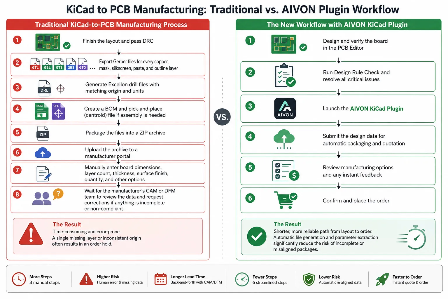
Traditional Gerber Workflow vs AIVON KiCad Plugin Workflow
Traditional workflow
Design → run DRC → plot Gerbers → generate drills → package ZIP → upload to manufacturer website → wait for DFM feedback → correct and re-upload if needed. Every manual step introduces the possibility of missing a layer or using inconsistent settings.
AIVON KiCad Plugin workflow
After the design is complete, the AIVON KiCad plugin can package the necessary manufacturing files and connect directly to the quotation and order process. This reduces repetitive file handling and the chance of uploading an incomplete set. The files still undergo professional manufacturing validation, but the path from layout to review is shorter and less error-prone.
How AIVON Helps KiCad Users Prepare Manufacturing-Ready Designs
Once the Gerber and drill files are generated, the next critical step is manufacturing validation. AIVON's engineering team reviews the submitted data for completeness, layer alignment, drill accuracy, and process compatibility before production begins. Feedback is provided early so corrections can still be made in KiCad rather than after boards have been fabricated.
The combination of a disciplined export process inside KiCad and professional engineering review significantly reduces the risk of holds or respins. Automated design submission tools further streamline packaging and quotation, allowing engineers to spend less time on file logistics and more time on the design itself.
Correct Gerber and drill export is the final engineering step that turns a KiCad design into a manufacturable product. Follow the preparation checklist, generate the complete layer set with consistent origins, verify everything in a viewer, and you will eliminate the majority of common factory rejects. When combined with professional manufacturing validation, the path from layout to finished boards becomes predictable and reliable.
FAQ
Q1: Do I need to export both top and bottom solder mask and silkscreen layers even for a single-sided board?
A1: Yes. Most manufacturers expect the complete layer set. Omitting the unused side can cause the CAM system to reject the job or assume incorrect defaults.
Q2: Why do my copper planes appear empty in the Gerber viewer?
A2: Copper zones were not refilled before plotting. Always press B (Fill All Zones) immediately before generating Gerbers.
Q3: Should drill files use the same origin as the Gerber files?
A3: Absolutely. Set the Drill/Place File Origin once and enable "Use drill/place file origin" in both the Plot and Drill dialogs. Mismatched origins are the most common cause of shifted holes.
Q4: What is the safest file-naming convention for manufacturers?
A4: Use the Protel-style extensions offered by KiCad (.gtl, .gbl, .gts, .gbs, .gto, .gbo, .gm1 or .gko for outline, .drl for drills). These are widely recognized.
Q5: Can I send the native KiCad board file instead of Gerbers?
A5: Almost never. Fabrication systems are built around Gerber and Excellon data. Always supply the plotted manufacturing files.