Many KiCad boards pass electrical checks yet still suffer from noise, voltage drops, or manufacturing rejects. One frequent cause is poorly implemented copper zones: incomplete ground planes, incorrect clearances, missing thermal reliefs, or zones that simply refuse to fill. Copper zones are not decorative fills—they are functional elements that determine return paths, current capacity, heat dissipation, and fabrication yield.
This guide explains how copper zones work in KiCad, how to create reliable ground and power planes, which settings actually matter, and how to solve the most common problems before they reach the manufacturer. The goal is to help you pour copper that improves layout efficiency and survives real fabrication and assembly.
What Are Copper Zones?
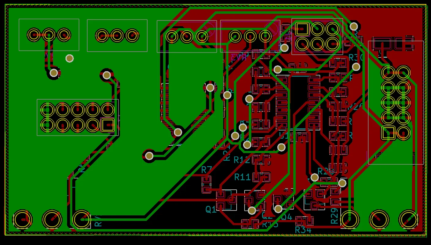
A copper zone (also called a copper pour or filled zone) is a polygonal area on a copper layer that KiCad automatically fills with copper connected to a specific net. The most common uses are solid ground planes and power distribution planes.
Copper zones are widely used because they provide low-impedance return paths, reduce electromagnetic interference, improve thermal performance, and simplify routing of power and ground. In multilayer boards they form the backbone of the power-delivery network. Even on two-layer boards a well-designed ground zone dramatically improves signal integrity compared with a sparse hatched or unfilled board.
Creating Copper Zones in KiCad
Adding Copper Areas
In the PCB Editor, select the Copper Zone tool (or press Ctrl+Shift+Z). Draw a closed outline that covers the area you want to fill. The outline can follow the board edge or be limited to a specific region. After drawing, the zone properties dialog opens.
Assigning Nets
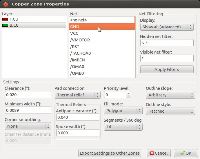
Assign the correct net—usually GND for a ground plane or a power net such as +3V3 or +5V. KiCad will connect the zone only to pads and vias that belong to that net. Leaving the net unassigned produces an isolated copper area that serves no electrical purpose and can create manufacturing problems.
Setting Layer Options
Choose the copper layer (F.Cu, B.Cu, or an internal layer). For multilayer boards you can create mirrored zones on multiple layers. Enable "Filled" and set the fill priority if several zones overlap. Higher-priority zones are filled first and can cut lower-priority zones.
Practical tip: start with a board-outline zone for the main ground plane, then add smaller zones only where needed for local power or isolation. Keep the outline slightly inside the board edge to satisfy the manufacturer's minimum copper-to-edge clearance.
Ground Plane Design with Copper Zones
GND Plane Strategy
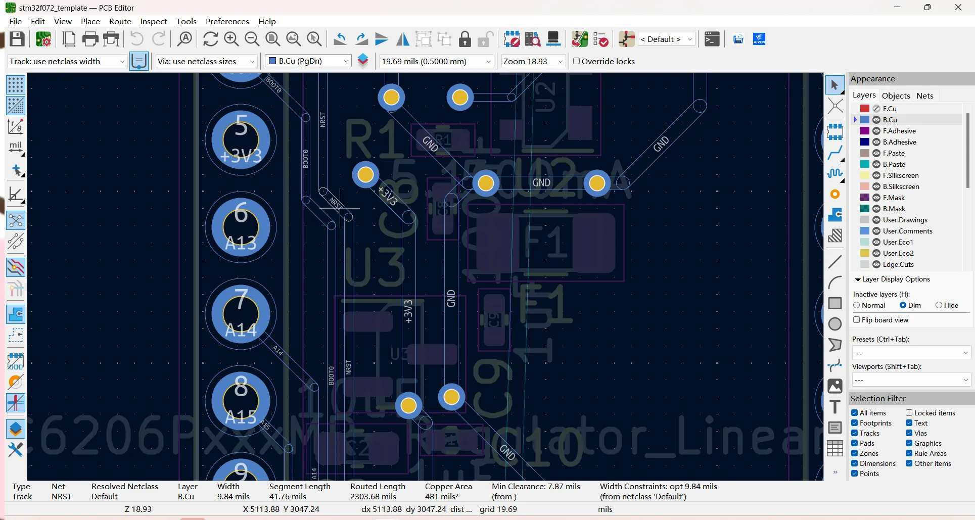
A continuous ground plane is the single most effective way to improve signal integrity and reduce EMI. On two-layer boards place the primary ground zone on the bottom layer and keep signal routing on the top. On four-layer (or higher) boards dedicate at least one internal layer to an unbroken ground plane.
Keep the ground plane as solid as possible. Avoid long slots or large openings that force return currents to detour. When a trace must cross a split, provide a nearby stitching via so the return path stays short.
Power Distribution Considerations
Power zones can be used for high-current rails, but they should never replace proper decoupling. Place decoupling capacitors close to the pins they serve and connect them to the power zone with short, wide traces or multiple vias. For mixed-signal designs consider separate analog and digital ground zones that meet at a single point near the power entry.
Manufacturing perspective: large unbroken copper areas help heat dissipation and reduce the risk of etching undercut. However, extremely large solid copper regions on outer layers can cause board warpage during reflow if the copper distribution is unbalanced between top and bottom.
Copper Zone Settings Explained
Clearance
Clearance is the minimum distance the zone keeps from pads, tracks, and vias that do not belong to its net. Set this value according to your manufacturer's minimum copper-to-copper spacing. Too small a clearance creates DRC errors and potential shorts; too large a clearance leaves unnecessary gaps that fragment the plane.
Thermal Relief
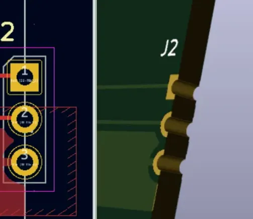
Thermal reliefs are the spoke-like connections between a pad and the surrounding zone. They limit heat flow during soldering so that through-hole or large SMD pads can still be soldered without excessive iron time. For most signal and low-power pads, use the default thermal-relief spokes. For high-current power pads, consider solid connections (no thermal relief) or heavier copper so the pad can carry the required current without overheating.
Fill Options
- Minimum thickness: prevents thin copper slivers that are hard to etch reliably.
- Pad connections: choose thermal relief, solid, or none.
- Fill type: solid is preferred for electrical performance; hatched is sometimes used for flexible circuits or to reduce copper weight.
- Remove islands: eliminates unconnected copper scraps that serve no purpose and can cause fabrication issues.
Always re-fill the zones after changing settings or after moving components. An outdated fill is one of the most common sources of "copper not filling" complaints.
Common Copper Zone Problems
Copper Not Filling
The most frequent causes are:
- The zone outline is not closed.
- The assigned net has no pads or vias inside the zone.
- "Filled" is disabled or the zone is set to a higher-priority zone that completely covers it.
- Clearance or minimum-thickness settings are so large that no copper can be poured.
Solution: verify the outline is closed, confirm the net assignment, lower the clearance temporarily, and click "Fill All Zones."
Clearance Issues
Zones that leave large gaps around every pad indicate clearance values that are too conservative for the design rules. Zones that produce DRC errors of "copper too close" indicate clearance values that are too aggressive for the manufacturer. Match the zone clearance to the board's design-rule clearance.
Manufacturing Concerns
Unconnected copper islands, copper too close to the board edge, or unbalanced copper distribution between layers can cause etching problems, warpage, or registration issues. Always run a full DRC after filling zones and inspect the Gerber output in a viewer. Confirm that thermal reliefs are present where needed and that solid connections are used only for pads that can tolerate the extra heat during soldering.
When zones and the rest of the layout are clean, generate the manufacturing files. Designing copper zones inside the fabricator's process limits and delivering a complete, verified package is the most reliable way to avoid production delays.
Copper zones are one of the highest-leverage tools in KiCad. Used correctly they improve electrical performance, thermal behavior, and manufacturing yield at the same time. Used carelessly they introduce noise, soldering difficulties, and fab rejects. Master the creation process, the critical settings, and the common failure modes, and your ground and power planes will become an asset rather than a source of last-minute fixes.
FAQ
Q1: How do I create a ground plane in KiCad?
A1: Use the Copper Zone tool, draw an outline covering the desired area, assign the GND net, select the appropriate copper layer, set clearance and thermal-relief options, then fill the zone. Re-fill after any component or rule changes.
Q2: Why is my copper zone not filling in KiCad?
A2: Common causes include an open outline, wrong or unassigned net, disabled fill option, or clearance/minimum-thickness values that leave no room for copper. Check these settings and click "Fill All Zones."
Q3: Should I use thermal reliefs on all pads connected to a copper zone?
A3: Use thermal reliefs for most signal and low-power pads to make soldering easier. For high-current power pads, solid connections are often better so the pad can carry the required current without excessive heating.
Q4: What clearance should I set for copper zones in KiCad?
A4: Match the zone clearance to your manufacturer's minimum copper-to-copper spacing and to the board's design-rule clearance. Values that are too tight create DRC errors; values that are too loose fragment the plane.
Q5: Do copper zones affect PCB manufacturing?
A5: Yes. Large unbalanced copper areas can cause warpage, copper too close to the edge can violate fab rules, and missing thermal reliefs can make soldering difficult. Always run DRC after filling and verify the Gerbers before ordering.