Over the past few decades, PCB aesthetics and practices have shifted dramatically. Beyond shrinking form factors, one of the most visible changes is the widespread use of copper pours—tool-generated polygon fills that occupy the unused areas between PCB traces. Why did this practice become so common, and does every PCB truly need a full-board copper pour?
From Early Personal Computers to Modern Maker Boards
In the early 1980s, a typical PCB in a home computer looked markedly different from today's designs. Large through-hole components, long trace runs, and sparse use of copper fills were the norm. By the late 2000s, even hobbyist-friendly platforms started showcasing dense SMT layouts and extensive ground fills.

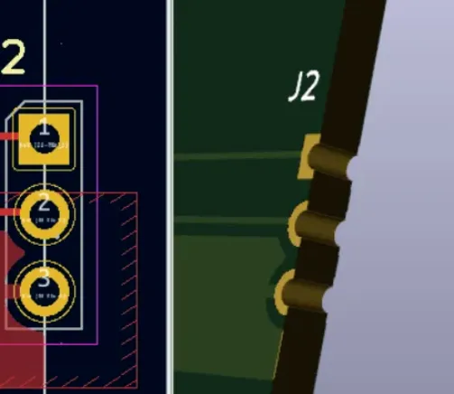
Figure 1 | Amstrad CPC 464 motherboard detail

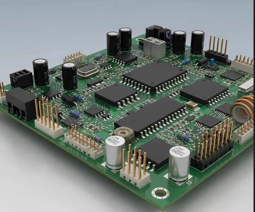
Figure 2 | Arduino Uno R3 close-up
Beyond miniaturization, three factors accelerated the adoption of copper pours:
- Signal-integrity considerations. In high-speed electronics, continuous reference planes and controlled return paths improve signal integrity. For smartphones, PCs, and other high-end products, this is essential.
- Regulatory pressure. Starting in the 1980s, the FCC began applying 47 CFR Part 15 (unintentional radiator rules) broadly to computing equipment. As compliance testing became mandatory and costly, designers adopted practices—such as continuous ground pours—that reduce radiated emissions and increase the likelihood of passing on the first try.
- Design culture and aesthetics. As techniques spread from professional to hobbyist circles, boards with pours and planes came to be seen as modern and "proper," even when the technical need wasn't clear.
Before answering whether your PCB needs a full-board copper pour, it helps to understand what copper pours actually do in electromagnetic terms.
A Short Detour: Common-Mode Chokes and Field Coupling
While electrons move within conductors, the energy transfer in circuits flows through electromagnetic fields surrounding those conductors. Materials like ferrites interact with these fields—via their high magnetic permeability and loss characteristics—introducing impedance for certain frequency components. As the ferrite absorbs magnetic field energy, it resists rapid changes in current until a new steady state is reached. This is the basis of inductive behavior.
A common and useful implementation is the common-mode choke. In its simplest form, two conductors are routed through a ferrite core in the same direction. More compact versions use a toroidal core with multiple turns per conductor.

Figure 3 | Conceptual diagram of a common-mode choke
Two current cases illustrate why this is useful:
- Common-mode current. When equal currents flow in the same direction on the two conductors, their magnetic fields reinforce within the core. The device acts like an inductor for the common-mode component: DC passes freely, but high-frequency components see increasing inductive reactance with frequency, reducing noise currents.
- Differential-mode current. When equal and opposite currents flow (as in a differential pair or supply +/? wires), the magnetic fields largely cancel in the core. The device then presents little impedance to the intended signal currents.
This is why common-mode chokes help mitigate RF interference on long cables: coupled environmental noise tends to be common-mode and is selectively impeded by the choke, while the desired differential-mode signal is preserved.
Back to Copper Pours: Return Paths, Inductance, and Emissions
You do not need ferrite cores to encounter inductive behavior—PCB traces themselves have inductance. Consider a simple two-layer PCB: a single signal trace on the top layer, a copper pour or plane on the bottom layer, and two vias that connect the circuit at the ends.

Figure 4 | Simplified PCB structure with a top trace and bottom copper return
With a DC signal applied, the "forward" current is confined to the top-layer trace. In the bottom copper, the return current could theoretically spread widely, but in practice it follows the path of least resistance between the two vias—typically a straight line. As frequency increases, the inductive nature of the current loop becomes important. A trace's inductance L is often on the order of tens to hundreds of nanohenries, depending on length, geometry, and stackup.
The inductive reactance for a given frequency f and inductance L is:

At around 20 MHz, this can easily approach about 50 Ω for a modest loop inductance. That's significant for any high-edge-rate signal: the loop's impedance rises with frequency, and the circuit begins to behave like a radiating structure.
There is an important mitigating effect: if the return current in the bottom copper is constrained to flow directly under the top trace—i.e., the return path closely follows the forward path's projection—the loop area shrinks. The opposing magnetic fields from forward and return currents then largely cancel, leading to much lower loop inductance and impedance. This is analogous, in effect, to the "field cancellation" that makes common-mode chokes transparent to differential currents.
Two practical problems follow from this physics:
- Large loop area causes higher impedance and radiation. If the forward and return paths are separated, the loop area grows and the path impedance increases. More energy is coupled into free space as electromagnetic radiation, which can degrade signal quality and increase the risk of failing emissions tests.
- Unintended current paths cause crosstalk and instability. If nearby "victim" traces or device structures offer an alternative return path (even through an IC body or package), return current may detour along those routes. That unpredictability can introduce noise, timing errors, or susceptibility to interference.
So, Do You Need a Full-Board Copper Pour?
Not necessarily. A copper pour is a convenient way to provide a continuous, low-impedance return path that tends to follow traces and minimize loop area, but it's not the only solution. Meticulous manual routing with deliberate return paths can also work. However, in many practical designs, a well-executed copper pour is faster and less error-prone than crafting a dedicated return path for each net or bus.
Regardless of the approach, design carefully. Discontinuities in the copper pour—splits, narrow necks, or voids—can force return currents to detour, degrading the return path quality and increasing loop area.

Figure 5 | Discontinuous pour causes a poor return path
Copper pours can also hide power-distribution shortcomings. For example, consider a device with a supply pin fed via a long, meandering positive rail while the ground pin enjoys a short, direct return. The positive supply path inductance will be high, and the loop can be unnecessarily large.

Figure 6 | Long positive supply path to a device pin
Some designers address these issues by moving to a four-layer stackup and dedicating the two inner layers to solid GND and Vdd planes. That is technically effective but increases manufacturing cost. Whether it's justified depends on your performance and compliance targets, board size constraints, and volume.
Planes, Inductance, and Parasitic Capacitance
Power and ground planes—or extensive copper pours—reduce loop inductance and improve return-path control. They also increase parasitic capacitance between conductors and the reference plane. For digital systems, this added capacitance is often benign or even desirable: it improves decoupling, stabilizes supply rails, and can modestly damp very high-frequency noise.
In analog circuits, the extra capacitance can be problematic. For example, in an op-amp feedback network, a few picofarads of unintended capacitance across a high-value resistor or into a sensitive node can reduce phase margin, alter the transfer function, or introduce peaking. When routing precision analog loops near planes, pay close attention to spacing, guard traces, and parasitic models.
Practical Guidance by Application
- General embedded designs. For projects built around microcontrollers such as ESP32 or 8-bit AVR devices, or using single-board computers for moderate-speed I/O, treat copper pours as a practical aid rather than a universal rule. Aim for continuous return paths under critical signals, avoid splits under high-edge-rate lines, keep supply loops tight, and place decoupling capacitors intelligently. You typically don't need to over-engineer these boards to the same degree as a high-speed backplane.
- High-speed interfaces. When dealing with interfaces like MIPI-DSI or USB 3.0 and above, the demands change. Controlled impedance, continuous reference planes, tight coupling of differential pairs, short and direct return paths, and careful management of plane transitions become essential. Here, full-board pours and well-planned layer stacks are not optional—they are part of the signal-integrity budget.
In short, copper pours are a powerful tool for managing return currents and reducing loop inductance, which in turn improves signal integrity and helps with EMI/EMC compliance. But they are not a substitute for thoughtful routing, power-distribution design, and stackup planning. Use them deliberately, avoid discontinuities, and recognize when a more advanced layer stack is warranted for your application.
As with many PCB practices, context matters. Let the electrical requirements—edge rates, interface types, compliance targets—drive your decision to pour copper across the entire board or to route selective, well-controlled return paths instead.