PCB Trace Width Explained: How Wide Should Your Traces Be?
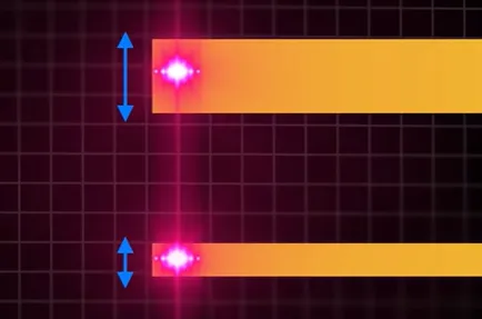
This short video demonstrates why two PCB traces carrying the same current behave differently based on width. Every copper trace has resistance that generates heat under load. A wider trace lowers resistance and reduces temperature rise for the same current, copper thickness, and ambient conditions.
Trace width selection depends on more than current alone. Copper thickness (commonly 1 oz or 2 oz), allowable temperature rise (often 10–20 °C), and whether the trace is on an outer or inner layer all influence the required cross-section. Outer layers dissipate heat more effectively than inner layers surrounded by dielectric, so internal traces typically need greater width for equivalent current capacity.
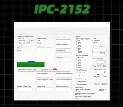
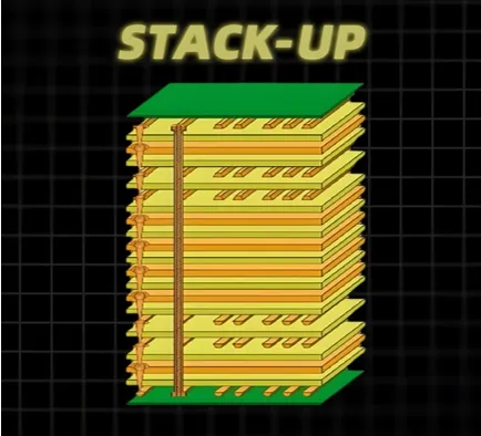
The recommended starting point is an IPC-2152-based trace-width calculator. Enter current, copper thickness, layer location, and temperature-rise limit to obtain a preliminary width. Long power traces then require voltage-drop checks, and the final design must be verified against the actual stack-up and fabricator limits. For high-speed signals, controlled impedance further constrains width based on dielectric height and copper weight.
Proper sizing prevents overheating, excessive voltage drop, and reliability issues in applications ranging from power supply PCBs to dense 4-layer PCBs and higher-current designs that may benefit from heavy copper PCBs. Calculate first, then verify against manufacturing constraints rather than relying on rules of thumb alone.
Key Highlights
- Wider traces reduce resistance and temperature rise for a given current; outer-layer traces cool better than internal traces of the same cross-section.
- IPC-2152 calculators provide a reliable starting width using current, copper thickness, layer location, and allowable temperature rise.
- Always verify voltage drop on long power traces and confirm the chosen width against stack-up impedance needs and fabricator minimum/maximum limits.
Why Trace Width Determines Resistance and Temperature Rise
Current flowing through a copper trace produces I²R heating. Resistance scales inversely with cross-sectional area (width × thickness), so a wider or thicker trace generates less heat for the same current. Under identical conditions, the narrower of two traces will run hotter and exhibit greater voltage drop over distance.
Temperature rise is not solely a function of current and area. Outer layers benefit from convection to air and can often tolerate higher current density before reaching a given rise. Internal layers are thermally isolated by prepreg and core dielectric, requiring larger area to stay within the same limit. Nearby copper pours or planes can further improve heat spreading, an effect accounted for more thoroughly in IPC-2152 than in older charts.
Undersized traces create reliability risks: elevated local temperatures accelerate copper oxidation or delamination, increase resistance over time, and can lead to thermal runaway under continuous load. In compact industrial control PCBs or sealed enclosures, even moderate rises compound ambient temperature and component self-heating.
A practical starting observation is that many engineers treat roughly 10 mil per amp on 1 oz outer copper at ~10 °C rise as a quick estimate, then refine with calculation. This rule is approximate and does not replace layer-specific verification.
Key Inputs for IPC-2152 Trace Width Calculation
IPC-2152 is the current industry reference for determining conductor current-carrying capacity. It incorporates test data that consider copper weight, layer position, board thickness, and proximity to planes, producing more realistic results than purely formula-based older standards for many designs.
Required inputs are straightforward: continuous or RMS current, copper thickness (0.5 oz, 1 oz, 2 oz, or heavier), layer location (external or internal), and maximum allowable temperature rise above local ambient. Calculators return a minimum width; designers then add margin for manufacturing tolerance, transient peaks, and long-term aging.
Example starting points for 1 oz copper and 10 °C rise (approximate, always recheck with a validated tool):
| Current | External Layer Width | Internal Layer Width |
|---|---|---|
| 1 A | ~15–25 mil | ~35–50 mil |
| 2 A | ~40–50 mil | ~65–80 mil |
| 3 A | ~60–70 mil | ~100–120 mil |
| 5 A | ~100–130 mil | ~180–220 mil |
Internal widths are typically 1.5–2× external for the same conditions because of poorer heat dissipation. Higher copper weight reduces the required width proportionally; moving from 1 oz to 2 oz roughly halves width for the same current and rise.
When calculated widths become impractical for routing density, options include increasing copper weight, using heavy copper PCB construction, or distributing current across multiple layers or a plane. For high-current paths in new energy PCBs or motor drives, heavy copper often proves more space-efficient than extremely wide 1 oz traces.
After obtaining the calculator result, confirm it against the specific stack-up. Dielectric thickness, copper coverage, and airflow all influence real-world temperature. Prototype thermal measurements under load provide the final validation.
Voltage Drop, Stack-Up Verification, and Controlled Impedance
Temperature rise is only one constraint. On long power traces, voltage drop (I × R) can become the limiting factor even when heating is acceptable. Trace resistance is calculated from resistivity, length, and cross-sectional area; designers commonly target less than 3–5 % of supply voltage at maximum load.
Because area = width × thickness, increasing either dimension lowers drop. Copper pours or solid planes are usually preferred over long traces for high-current distribution, as they provide both lower resistance and better heat spreading. In multilayer boards, dedicating an internal layer to a power plane and stitching with multiple vias reduces both drop and hot spots.
For high-speed or high-frequency signals, controlled impedance imposes an independent width requirement. Characteristic impedance depends on trace width, copper thickness, dielectric height to the reference plane, and dielectric constant. A width that satisfies current capacity may not match the target impedance (commonly 50 Ω single-ended or 100 Ω differential). In high frequency PCBs or Rogers material designs, impedance-driven widths take priority, and current capacity is verified separately or addressed with thicker copper.
Neck-downs—short sections of reduced width to pass between pins or vias—must be evaluated at the narrowest point for current rating. The thermal length of the constriction still matters, but the minimum cross-section sets the continuous-current limit. HDI designs frequently encounter this trade-off; maintaining consistent width where possible reduces both impedance discontinuities and local heating.
Always run the final widths through the fabricator's DFM check. Stack-up dielectric tolerances and etch compensation can shift both impedance and effective copper area.
Manufacturing Limits and DFM Best Practices for Trace Width
Fabricators publish minimum trace/space capabilities that vary with copper weight and process. Standard 1 oz FR4 typically supports 4–6 mil minimum features economically; tighter geometries increase cost and reduce yield. Heavier copper (2 oz and above) requires wider minimum features because of etch undercut.
A calculated width that falls below the process capability cannot be produced reliably. Conversely, excessively wide traces consume routing channels and can complicate solder-mask registration or component placement. For dense layouts, designers often use the calculated minimum plus a 20–50 % margin, then adjust copper weight or layer count if space is insufficient.
Etch factor causes finished trace width to differ slightly from the designed width; high-volume or tight-tolerance boards account for this in CAM compensation. Acute angles or sudden width changes can trap etchant and create reliability defects, so 45-degree or curved transitions are preferred.
In PCB prototype runs, it is common to oversize power traces slightly to provide margin while confirming actual temperature rise. For production, align the design with the fabricator's preferred copper weights and stack-ups to avoid cost premiums associated with non-standard features.
When standard copper cannot meet both current and density targets, heavy copper PCBs or specialized constructions (for example, selective heavy copper or embedded copper) become practical alternatives. These require early discussion of plating, lamination, and thermal-via strategies.
Practical Selection Guide for Power and Signal Traces
Begin with the continuous or RMS current the net must carry under worst-case conditions. Choose an allowable temperature rise based on ambient, enclosure, and nearby heat sources—10 °C is conservative for many commercial designs; 20 °C is common when airflow or planes assist cooling.
Select copper weight appropriate to the overall board (1 oz standard, 2 oz for moderate power, heavier for high current). Run the IPC-2152 calculator for both external and internal placement, then decide layer assignment. Prefer outer layers or planes for high-current nets when possible.
Next, calculate voltage drop for the expected trace length and adjust width or switch to a pour if the drop is excessive. For impedance-controlled nets, lock the width required by the stack-up first, then confirm current capacity.
Finally, compare the resulting geometry against fabricator minimums, preferred spacing, and panelization constraints. Add margin for etch tolerance and transient peaks. Document the assumptions (current, rise, copper, layer) so subsequent reviews or engineering change orders remain consistent.
This sequence—calculate, check drop and impedance, verify against manufacturing limits—avoids both undersized traces that overheat and oversized traces that waste space or inflate cost.
FAQ
Q1: What trace width do I need for 1 A on 1 oz copper?
A1: For a 10 °C rise on an external 1 oz layer, most IPC-2152 calculators return approximately 15–25 mil. Internal layers typically require 35–50 mil or more for the same conditions. Always confirm with a calculator using your exact temperature-rise limit and stack-up.
Q2: How much wider must an internal trace be compared with an external trace?
A2: Internal traces usually need 1.5–2× the width of an external trace for the same current, copper thickness, and temperature rise because surrounding dielectric limits heat dissipation. Nearby planes can reduce this difference.
Q3: When should I use heavier copper instead of a wider trace?
A3: When the calculated width for 1 oz copper exceeds available routing space or creates excessive voltage drop, increasing to 2 oz or moving to a heavy-copper construction reduces the required width while maintaining current capacity. This is common on power-distribution and high-current boards.
Q4: Does controlled impedance change the required trace width?
A4: Yes. Impedance targets fix width based on dielectric height, copper thickness, and dielectric constant. The impedance-driven width must still be checked for current capacity; if it is insufficient, options include thicker copper, a different stack-up, or relocating the net.
Q5: What is a practical temperature-rise limit for most designs?
A5: Many commercial and industrial designs start with 10 °C rise for conservative thermal margin or 20 °C when planes and airflow provide additional cooling. The limit should reflect local ambient temperature, enclosure conditions, and nearby component heat, not simply room temperature.
Two PCB traces. Same current. Why does width matter?
Watch what happens when current flows through copper.
Every trace has resistance, which generates heat.
Under the same conditions, a wider trace has lower resistance.
But how wide should your trace actually be?
It depends on more than current.
Copper thickness, allowable temperature rise, and whether the trace is on an outer or inner layer all matter.
Here's how to choose: use a trace-width calculator based on IPC-2152.
Enter your current, copper thickness, layer location, and allowable temperature rise to estimate a starting width.
Then check voltage drop on long power traces and verify your design against your actual PCB stack-up and manufacturing limits.
For high-speed signals, you also need controlled impedance.
Don't guess. Calculate, then verify.