 00:59
00:59
PCB Trace Routing
PCB trace routing is a fundamental aspect of printed circuit board (PCB) design, involving the strategic placement and connection of conductive paths that link electronic components. This process ensures reliable signal transmission, power distribution, and overall circuit performance, making it essential for engineers, hobbyists, and professionals tackling projects from simple prototypes to complex multilayer boards. By mastering PCB trace routing, designers can minimize issues such as electromagnetic interference, signal degradation, and thermal hotspots, which are common challenges in high-speed or high-density applications. For those searching for insights on PCB trace routing, this tag compiles resources that delve into practical techniques and best practices. Key topics include selecting appropriate trace widths based on current requirements, implementing differential pair routing for noise reduction, and adhering to design rules for manufacturability. Whether you are optimizing layouts for RF circuits, ensuring compliance with standards like IPC-2221, or troubleshooting routing errors in software tools such as Altium or KiCad, the articles here offer actionable guidance. For instance, understanding via placement and ground plane strategies can significantly enhance board reliability and reduce prototyping iterations. Exploring the content under this tag provides a pathway to refine your skills through real-world examples and case studies. From beginner tutorials on basic single-layer routing to advanced discussions on automated routing algorithms, these materials equip you with the knowledge to create efficient, cost-effective PCBs. If you are designing for automotive, medical, or consumer electronics, applying these routing principles can lead to more robust and scalable solutions, ultimately streamlining your development process.
Video Guide

Technical Articles

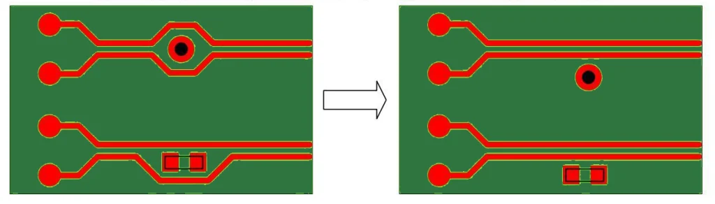
Can a 0 Ω Resistor Really Be Used as a Jumper? A Trap Many Engineers Have Hit
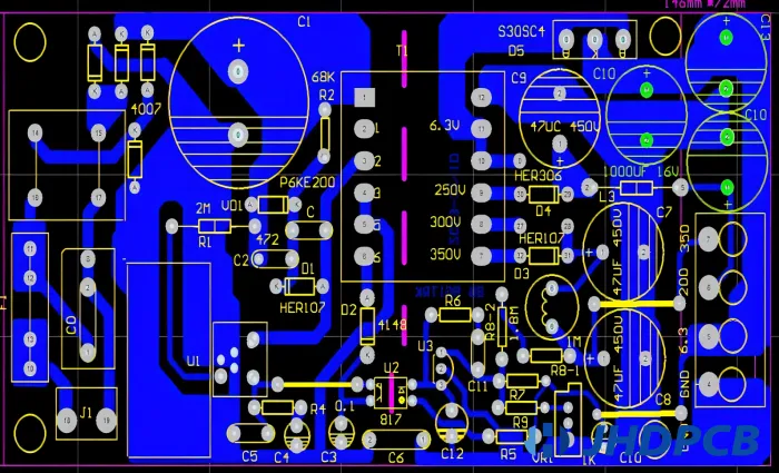
Cost Effective PCB Trace Routing: Strategies for Reducing Manufacturing Costs
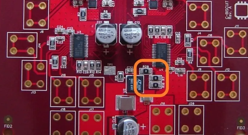
Zero Ohm Resistors vs. Jumpers: When to Use Which in Your PCB Design
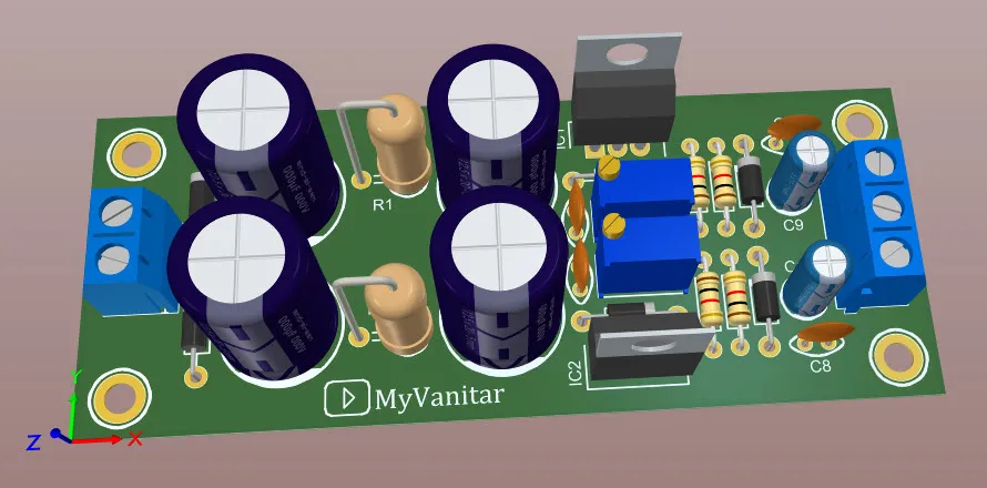
Best Practices for Power Supply PCB Trace Routing
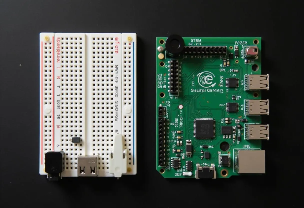
From Breadboard to PCB: Making Your Projects Permanent
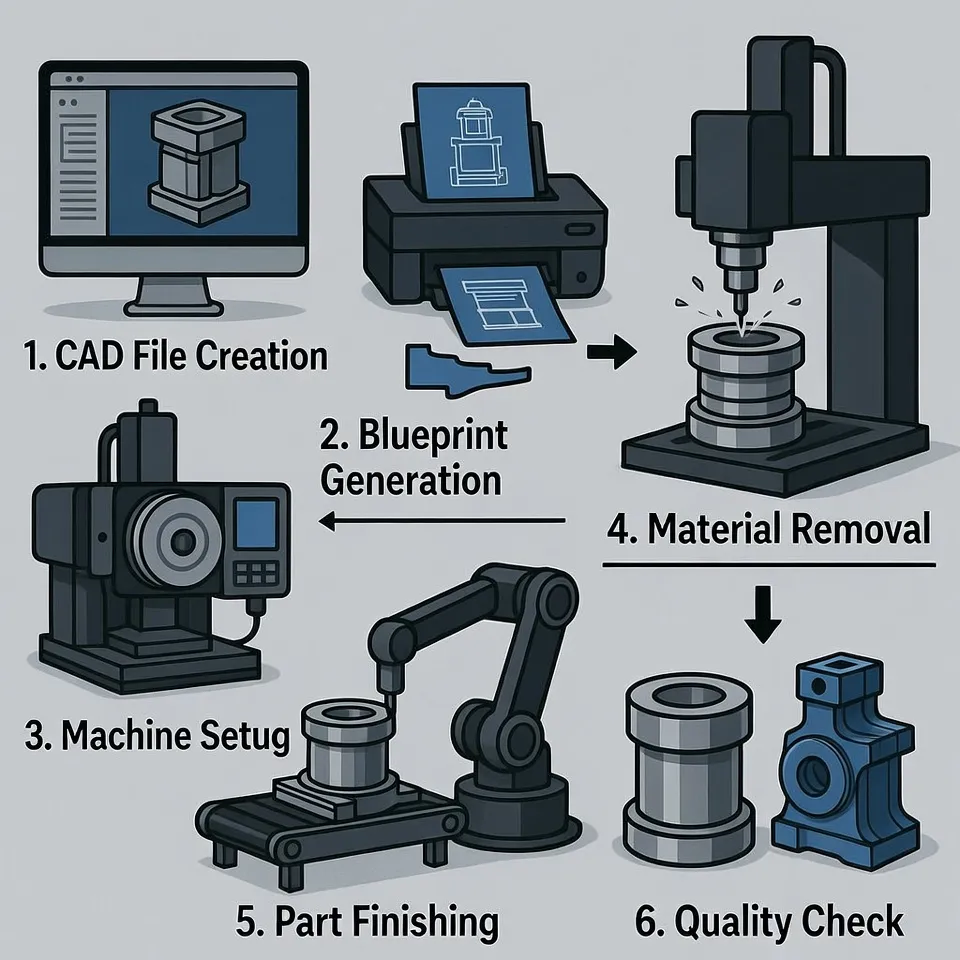
CNC Machining Process Explained: From CAD File to Finished Part
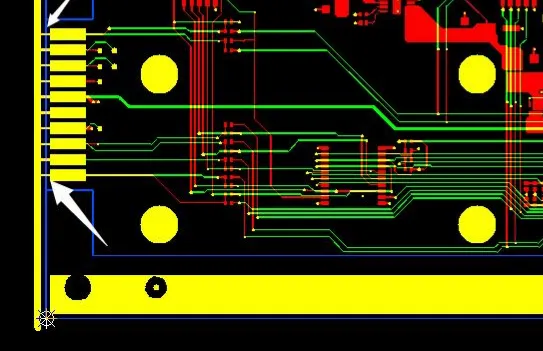
DFM Fixes for Non-Plated Slots, Gold Fingers & Trace Extensions in 4-Layer FR4 PCB
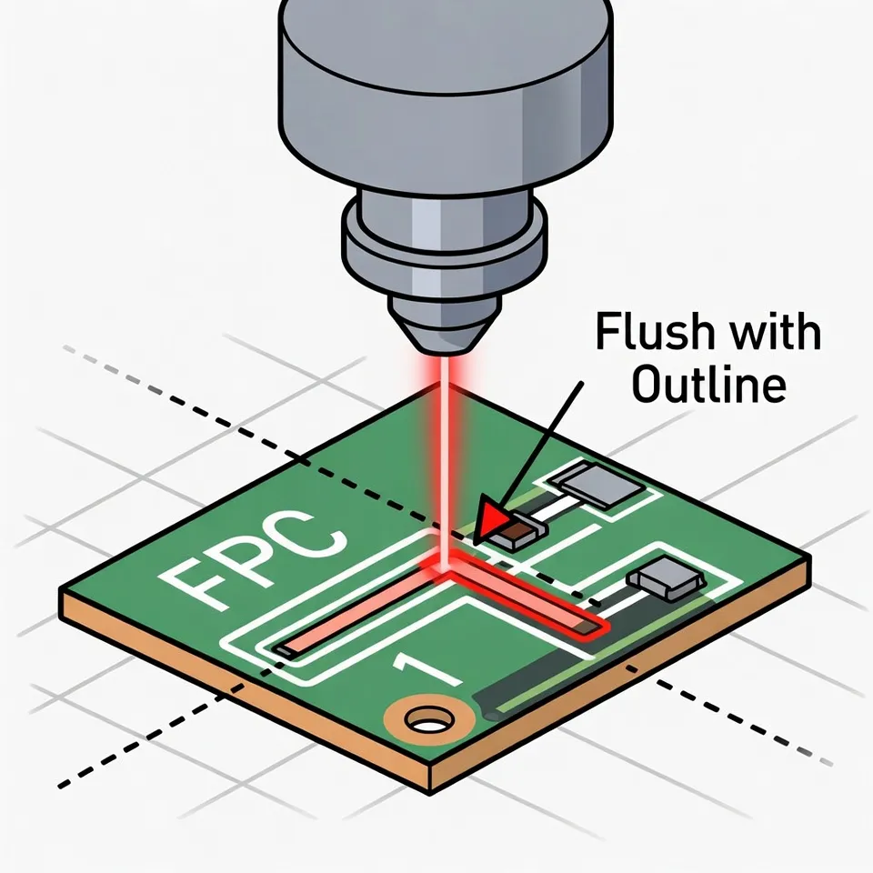
Why FPC Traces Flush with Outline Cause Laser Cutting Problems
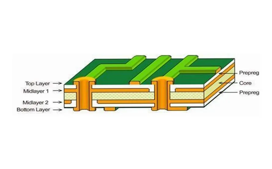
The Ultimate Guide to Connecting Components with Inner Layer Traces
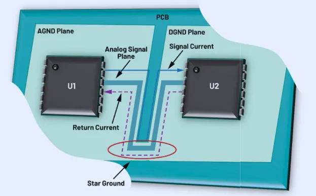
Mastering PCB Signal Routing for Crystal-Clear Audio Amplifiers
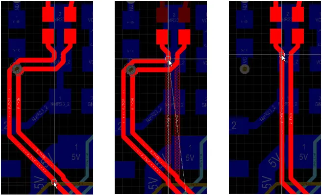
Maximizing Efficiency: Effective Strategies for PCB Routing
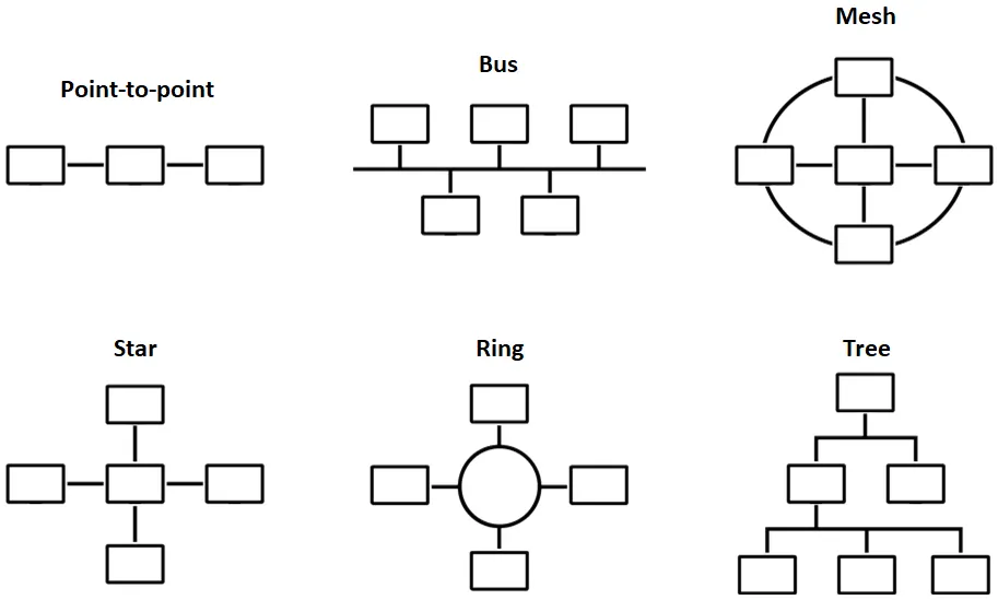
The Art of PCB Trace Routing: Topologies, Techniques, and Best Practices
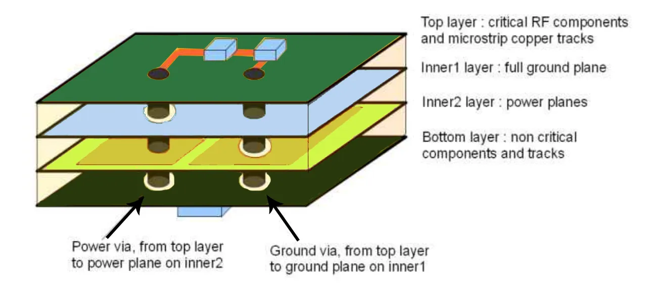
Routing Challenges and Solutions on 4-Layer PCBs
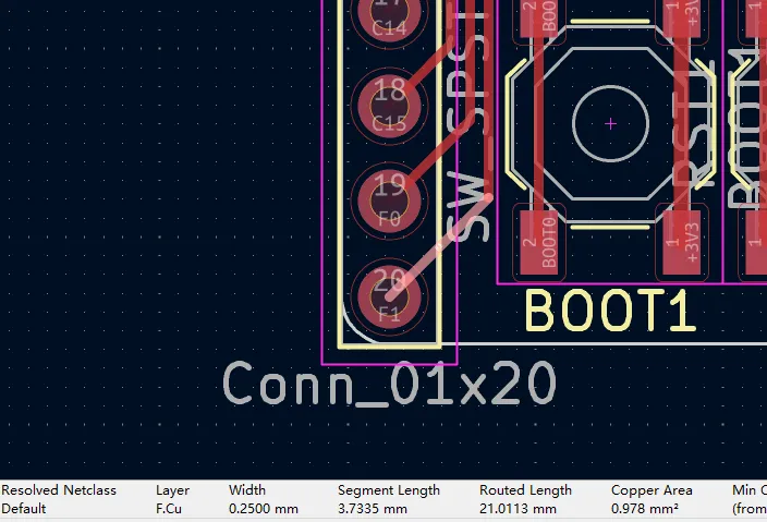
Choosing the Right Trace Width in KiCad: PCB Design Rules and Guidelines