Introduction
For electronic hobbyists diving into printed circuit board (PCB) design, understanding how to effectively use inner layer traces is a game changer. These conductive pathways, hidden within multilayer PCBs, play a critical role in connecting components while optimizing space and enhancing performance. Inner layer traces allow for denser layouts, improved signal integrity, and reduced electromagnetic interference, making them essential for complex projects. This guide explores the fundamentals of inner layer traces, their importance in PCB trace routing, and practical tips for connecting components. Whether you are designing a simple microcontroller board or a sophisticated gadget, mastering this technique can elevate your skills. Join us as we break down the technical principles and best practices to help you create efficient and reliable designs.
What Are Inner Layer Traces and Why Do They Matter
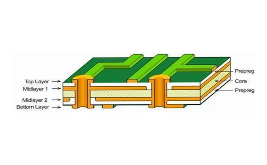
Inner layer traces are conductive copper pathways embedded within the internal layers of a multilayer PCB. Unlike surface traces on the top or bottom layers, these are sandwiched between insulating materials, often forming part of a four layer or higher stackup. They serve the same purpose as external traces, which is carrying electrical signals or power between components, but their placement inside the board offers unique advantages.
The significance of inner layer traces lies in their ability to maximize space. By moving connections to internal layers, hobbyists can free up surface area for additional components or reduce the overall board size. They also help in managing signal integrity by providing shorter paths and reducing noise through proximity to ground planes. For projects involving high speed signals or dense layouts, such as robotics or IoT devices, inner layer traces are indispensable. Additionally, they contribute to better thermal management by distributing heat across internal copper layers. Understanding their role is the first step toward creating compact and efficient PCB designs.
Technical Principles of Inner Layer Traces in PCB Design
The functionality of inner layer traces relies on the structure of multilayer PCBs. A typical four layer board consists of two outer layers for components and signals, and two inner layers often dedicated to power and ground planes or additional signal routing. Inner traces are etched onto these internal copper layers during manufacturing, then insulated by prepreg and core materials before being laminated together.
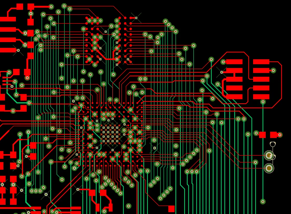
When connecting components using inner layer traces, vias play a crucial role. These small conductive holes link traces across different layers, allowing signals to transition from surface mounted components to internal pathways. The placement and type of vias, such as through hole or blind vias, impact the design's complexity and performance. Signal integrity is another key consideration. High speed signals routed on inner layers benefit from reduced crosstalk when adjacent to a ground plane, as the plane acts as a shield against interference.
Trace width and spacing on inner layers must also be carefully planned. Narrow traces may overheat under high current, while improper spacing can lead to signal coupling. Industry standards, such as IPC-2221B, provide guidelines for determining safe trace dimensions based on current and temperature rise. Hobbyists should adhere to these principles to ensure reliability.
Suggested Reading: How Does PCB Trace Width Affect Impedance?
Layer Stack-up Configurations for Optimal Inner Layer Routing
Choosing the right stack-up maximizes the value of inner layer traces. Common hobbyist-friendly configurations include:
- SIG-GND-PWR-SIG (classic 4-layer): Inner layers dedicated to solid ground and power planes provide excellent reference planes for outer signals, minimizing EMI and simplifying routing. Ideal for most microcontroller projects.
- SIG-GND-SIG-PWR: Places two signal layers adjacent to the ground plane for high-speed or sensitive analog routing on inner layers, with power on the bottom inner layer.
- 6-layer variants (e.g., SIG-GND-SIG-PWR-SIG-GND): Adds dedicated inner signal layers for complex designs while maintaining symmetric construction to control warpage below 0.75%.
Symmetric builds with low-CTE materials reduce manufacturing defects. Solid reference planes on inner layers are preferred over split planes to avoid return-path discontinuities
Best Practices for Connecting Components with Inner Layer Traces
For electronic hobbyists, routing inner layer traces to connect components can seem daunting, but following best practices simplifies the process. Below are actionable tips to achieve effective PCB trace routing while maintaining design quality.
- Plan Your Layer Stackup Early: Decide the purpose of each layer before routing. Typically, inner layers in a four layer board are used for power and ground to provide a stable reference for signals on outer layers. If additional signal routing is needed internally, ensure it does not interfere with these planes.
- Minimize Via Usage: While vias are necessary for connecting components to inner layer traces, excessive use can increase manufacturing complexity and cost. Route as many connections as possible on a single layer before transitioning through vias. When unavoidable, place vias strategically to avoid clutter.
- Maintain Consistent Trace Widths: Ensure that trace widths on inner layers match the current carrying requirements. Refer to standards like IPC-2221B for guidance on calculating appropriate widths to prevent overheating or voltage drops.
- Use Ground Planes Effectively: Position inner layer traces near a ground plane to reduce electromagnetic interference. This is especially important for high speed signals, as the ground plane helps maintain signal integrity by minimizing noise.For detailed calculations on trace dimensions, review our guide to how trace width affects impedance on inner layers.
- Avoid Overlapping Signals: When routing multiple signals on an inner layer, keep adequate spacing to prevent crosstalk. Standards such as IPC-6012E emphasize the importance of separation for reliable performance.
By applying these guidelines, hobbyists can create designs that balance functionality with manufacturability.
Impedance Control, Differential Pairs, and Signal Integrity on Inner Layers
Inner layers offer superior impedance control because traces form stripline structures (sandwiched between two reference planes) rather than microstrip. This configuration provides tighter impedance tolerance (±5–10% achievable) and lower crosstalk due to enclosed electromagnetic fields.
For differential pairs on inner layers, maintain tight coupling (edge-to-edge spacing ≈ trace width), equal lengths (±5 mil tolerance for multi-GHz signals), and continuous reference planes. Avoid vias in differential pairs when possible; when required, use back-drilled or blind vias to minimize stubs. Proper inner-layer routing can achieve >40 dB isolation between adjacent pairs in well-designed stacks.
Common Challenges and Solutions in Inner Layer Routing
Even with careful planning, routing inner layer traces can present challenges for hobbyists. One common issue is signal degradation due to long trace lengths or improper layer transitions. To address this, keep high speed signals as short as possible and avoid unnecessary layer changes. If a transition is needed, ensure vias are placed close to the component pads to minimize inductance. Proper via selection is essential when transitioning signals from surface components to inner layer traces in multilayer designs.
Another challenge is thermal management. Inner layer traces carrying high current can generate heat, which is harder to dissipate compared to surface traces. A solution is to increase trace width or add copper pours on inner layers to spread heat more evenly. Consulting IPC-2221B for current capacity guidelines is advisable.
Lastly, design rule violations can occur when spacing between traces is insufficient, leading to potential short circuits. Using design software with built in rule checking based on standards like IPC-A-600K helps identify and correct such issues before fabrication.
Tools and Techniques for Effective PCB Trace Routing
For hobbyists, selecting the right tools and techniques can make inner layer trace routing more manageable. Most modern electronic design automation software offers features to handle multilayer designs. These tools allow you to define layer stackups, assign specific functions to each layer, and automatically check for design rule compliance.
Start by sketching a rough schematic of component connections to identify which signals need inner layer routing. Once the schematic is ready, use the software's layer management feature to allocate traces accordingly. Many platforms provide visual aids to distinguish between layers, making it easier to track inner layer traces.
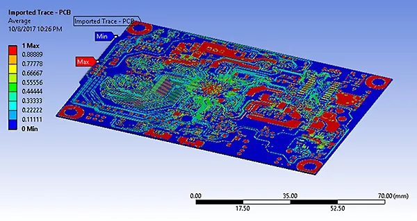
Manual routing is often necessary for critical signals to ensure optimal paths. However, for less sensitive connections, autorouting features can save time, though they should be reviewed for accuracy. Additionally, simulate your design for signal integrity and thermal performance if the software supports it. This step helps spot potential issues with inner layer traces before sending the design for fabrication.
Advanced Testing, Verification, and DFM for Inner Layers
Beyond visual inspection, use built-in Design Rule Checks (DRC) against IPC-2221B/IPC-6012 standards. For signal integrity, free tools like LTSpice or KiCad’s integrated simulator help model inner-layer behavior. Professional fabs offer cross-section analysis on test coupons to verify plating and registration.
DFM checks should confirm minimum inner trace spacing (typically 4–6 mil for standard processes), annular ring sizes (>6 mil), and symmetric copper distribution to prevent warping. In 2026, many low-cost services provide free DFM reports highlighting inner-layer issues before fabrication.
Real-World Case Studies and Lessons Learned
Case Study 1: IoT Environmental Sensor Node
A hobbyist redesigned a four-layer ESP32-based sensor from two-layer to SIG-GND-PWR-SIG stack-up. Moving power distribution and some SPI traces to inner layers reduced board size by 35%, lowered EMI enough to pass basic FCC pre-compliance, and improved battery life by minimizing noise-induced resets. Lesson: Early stack-up planning and ground-plane stitching vias were critical; autorouter cleanup took longer than expected but paid off in density.
Case Study 2: DIY Robot Arm Controller
A 6-layer board for stepper motor drivers used inner layers for high-current power traces (up to 3 A) and differential encoder signals. Inner-layer routing with 2 oz copper on power planes prevented thermal issues during prolonged operation. Differential pairs on inner stripline layers maintained clean signals despite nearby motor noise. Lesson: Thermal simulation in Fusion 360 caught a hot spot early; specifying exact trace widths in fab notes avoided manufacturing surprises.
Future Trends in Inner Layer Routing for 2026 and Beyond
In 2026, hobbyists increasingly access affordable HDI processes with microvias and any-layer interconnects, allowing even denser inner-layer routing through services like JLCPCB or PCBWay. AI-assisted routing plugins in KiCad and cloud tools automatically suggest optimal inner-layer paths while respecting impedance and thermal constraints. New low-loss dielectrics and embedded component techniques are trickling down to hobbyist budgets, while simulation tools with built-in IPC calculators make advanced inner-layer design more approachable than ever. Expect tighter integration between mechanical and electrical CAD for compact wearable and robotics projects.
Conclusion
Mastering the use of inner layer traces is a valuable skill for electronic hobbyists aiming to create compact and high performing PCB designs. These hidden conductive paths enable efficient connecting of components, optimize board space, and enhance signal integrity when used correctly. By understanding the technical principles behind multilayer stackups, adhering to best practices for PCB trace routing, and addressing common challenges, you can elevate the quality of your projects. Applying guidelines from recognized standards ensures reliability and manufacturability. As you experiment with inner layer traces, focus on careful planning and iterative testing to achieve the best results in your electronic endeavors.
FAQs
Q1: What are inner layer traces, and why should hobbyists use them in PCB designs?
A1: Inner layer traces are conductive paths within the internal layers of a multilayer PCB, used for connecting components. They help hobbyists save surface space, allowing for denser designs and smaller boards. Additionally, they improve signal integrity by reducing noise when placed near ground planes, making them ideal for complex or high speed projects.
Q2: How do I ensure proper PCB trace routing on inner layers as a beginner?
A2: Start by planning your layer stackup and assigning specific roles to each layer, such as power or signal routing. Use design software to visualize inner layer traces, maintain consistent trace widths, and minimize vias. Refer to standards like IPC-2221B for guidance on spacing and current capacity to avoid errors.
Q3: What challenges might I face when connecting components with inner layer traces?
A3: Common challenges include signal degradation from long traces, thermal issues with high current, and spacing violations. Address these by keeping traces short, increasing widths for current heavy paths, and using design rule checks based on standards like IPC-A-600K to ensure proper separation and reliability.
Q4: Can inner layer traces improve signal integrity in my hobbyist PCB projects?
A4: Yes, inner layer traces can significantly enhance signal integrity. Routing high speed signals on inner layers near a ground plane reduces electromagnetic interference and crosstalk. This setup stabilizes signals, making it a valuable technique for projects involving microcontrollers or wireless communication modules.
References
IPC-2221B — Generic Standard on Printed Board Design. IPC, 2012.
IPC-6012E — Qualification and Performance Specification for Rigid Printed Boards. IPC, 2020.
IPC-A-600K — Acceptability of Printed Boards. IPC, 2020.


