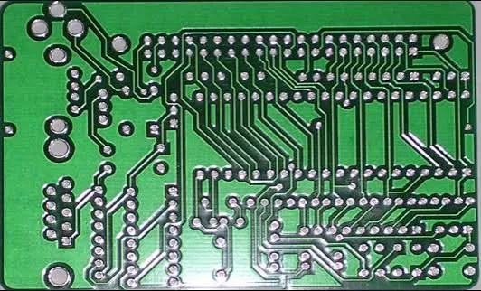
FPC trace too close to edge creates real headaches during laser routing. When traces sit flush with the final outline, even minor cutting variations turn into open circuits or exposed copper that invites shorts later. This isn't theoretical — it's a common DFM flag in flex production.
Laser Cutting Tolerance and Its Effect on Flush Traces
Laser cutting on flex circuits offers precision, but it still carries positional and kerf tolerances typically in the ±0.05 mm to ±0.1 mm range depending on the machine and material. When your copper trace runs exactly at the board outline, any slight offset cuts into the trace itself.
The laser beam removes material along a programmed path. On polyimide with copper, the cut edge can wander because of material tension release, web handling, or thermal expansion during the process. A trace sitting right on the edge has zero margin for these variations.

Why Designers Sometimes Place Traces Flush to the Edge
Tight space constraints drive this decision. In wearable devices, medical sensors, or slim automotive modules, every millimeter counts. Engineers push traces to the absolute limit to maximize routing density or meet mechanical bend requirements near the edge.
Sometimes it's for EMI shielding or to maintain controlled impedance right up to a connector. The layout looks perfect in CAD. But manufacturing reality hits when the panel moves to laser routing.
Actual Risks of Short Circuits and Exposed Copper
The most immediate failure is trace damage. Partial cuts create necking or complete opens. Even if the trace survives initial routing, the remaining copper at the edge becomes vulnerable.
Exposed copper along the cut edge oxidizes quickly. In humid environments or during assembly, this leads to dendrite growth or electrochemical migration. More critically, it raises the chance of solder bridging or conductive debris causing intermittent shorts during flexing.

Mechanical stress makes things worse. FPCs bend and fold in use. A trace right at the outline experiences higher strain concentration. Delamination or cracking follows, especially after repeated cycles.
In high-volume production, these issues compound. One panel with marginal clearance can scrap an entire lot when downstream testing catches the shorts or opens.
Coverlay and Solder Mask Interaction at the Edge
Coverlay registration adds another layer of tolerance. If the coverlay window or edge doesn't perfectly align with the laser cut, you get exposed copper or adhesive squeeze-out that interferes with the trace. Flush designs leave no room to accommodate this misalignment.
DFM Safe Distance Guidelines for FPC Traces to Outline
Standard practice calls for at least 0.15 mm clearance between the copper trace and the final laser-routed outline on flex circuits. For finer lines or higher reliability applications, 0.2 mm to 0.3 mm provides better margin.
This distance accounts for laser kerf width (typically 0.02-0.05 mm), positional tolerance, and coverlay overlap. It also gives room for any edge plating or protective treatments if needed.

Adjusting Your Layout for Reliable Laser Routing
Review your stackup and routing early. Move critical traces inward where possible. Use teardrops or neck-downs only away from the edge. For areas that truly need edge proximity, consider adding dummy copper or sacrificial traces that can absorb minor cutting variations.
Panelization strategy matters too. How the flex array sits on the carrier and the direction of laser travel can influence edge quality. Discuss this with your manufacturer during DFM review.
Long-Term Reliability Implications of Marginal Edge Clearance
A trace damaged during laser cutting may pass initial electrical test but fail in the field. Vibration, thermal cycling, and constant flexing accelerate crack propagation from the weakened edge.
Signal integrity suffers as well. Impedance discontinuities appear at the damaged section, especially noticeable in high-speed or RF flex applications. Return loss increases and crosstalk can jump.
From a manufacturing standpoint, consistent edge clearance improves yield dramatically. It reduces touch-up work, lowers scrap rates, and makes the overall process more repeatable across different production runs.
Practical Checks During Layout Review
Run a design rule check specifically for outline proximity. Measure minimum distance from all copper features to the final profile. Account for any bevels or special shaping in the flex design.
Share the gerber files with your CAM team early. They can simulate the laser path and highlight risky areas before committing to tooling.
Key Takeaways for Avoiding FPC Trace Too Close to Edge Issues
Respecting proper clearance between traces and the laser-cut outline prevents most of these problems. The FPC trace too close to edge, flex PCB outline short risk isn't worth the space savings in the long run.
Build the margin into your initial layout. It costs almost nothing in design time but saves significant headaches, cost, and reliability risks downstream. When in doubt, add a little more distance — your production team will thank you for it.
Next time you're routing a dense flex design, zoom in on those outline areas. A quick adjustment there can mean the difference between smooth production and weeks of troubleshooting.