










PCB Power Design Mistakes: Critical Errors to Avoid Before Routing
What This Video Covers
Power delivery problems are among the most common reasons beginner PCB designs fail after assembly. This video identifies the top power-related mistakes made before routing even begins and shows how to avoid them for stable, reliable boards.
The guide stresses accurately calculating total current requirements — including MCU, sensors, LEDs, and startup spikes — before selecting regulators. It explains the distinct roles of bulk capacitors versus decoupling capacitors and why a deliberate strategy is essential to prevent voltage drops under load.
Viewers learn why using a single via or thin trace for power pins creates high current density and inductance issues, and why simply pouring a power plane does not automatically solve return path, placement, or loop area problems.
These concepts apply directly to 4-layer PCB, multilayer PCB, and high-reliability designs used in IoT devices, industrial control systems, and automotive electronics. Proper power design before routing significantly improves signal integrity, thermal management, and overall product reliability.
Get an instant PCB quote or explore turnkey PCB assembly services and 4-layer PCB manufacturing for your next project.
Key Highlights
- Current Calculation: Always calculate total current draw including peak loads before selecting regulators — guessing leads to unstable power delivery.
- Capacitor Strategy: Bulk and decoupling capacitors serve different purposes; a deliberate placement strategy is required to maintain stable voltage under varying loads.
- Power Delivery Details: Multiple vias, proper return paths, and careful placement matter far more than simply adding a power plane.
Why Power Delivery Problems Cause Most Beginner PCB Failures
In real production environments, inadequate power distribution networks (PDN) frequently result in boards that pass initial power-up but fail under load, temperature cycling, or in the field. Issues like voltage droops, excessive ripple, and ground bounce manifest as random resets, erratic sensor readings, or complete system instability. These problems often trace back to decisions made before any signal routing begins.
From a manufacturing perspective, such designs lead to higher scrap rates, repeated engineering change orders (ECOs), and delayed time-to-market. CAM engineers commonly review layouts where power paths create hot spots detectable during thermal imaging or cause solder joint stress due to uneven current distribution. Early attention to PDN fundamentals prevents these costly downstream issues in multilayer stackups typical for IoT, industrial, and automotive applications.
Accurate Current Calculation and Regulator Selection
Always calculate total current draw including peak loads and inrush currents before selecting voltage regulators. Guessing or using datasheet typical values instead of worst-case scenarios (including startup transients, simultaneous switching, and future expansions) leads to undersized supplies and unstable power delivery.
In practice, add at least 20-50% margin depending on the application. For example, an MCU with 100mA average draw might spike to 300mA+ during boot or peripheral activation. Insufficient headroom causes regulators to drop out or enter protection modes, resulting in brownouts visible in production testing.
Table: Typical Current Margin Recommendations for Common Applications
| Application | Average Current | Recommended Margin | Key Considerations |
|---|---|---|---|
| IoT Sensors | 50-200mA | 30-50% | Battery life and sleep currents |
| Industrial Control | 0.5-2A | 20-40% | Load transients and EMC |
| Automotive Modules | 1-5A | 30-50% | Temperature extremes and vibration |
Bulk Capacitors vs Decoupling Capacitors Strategy
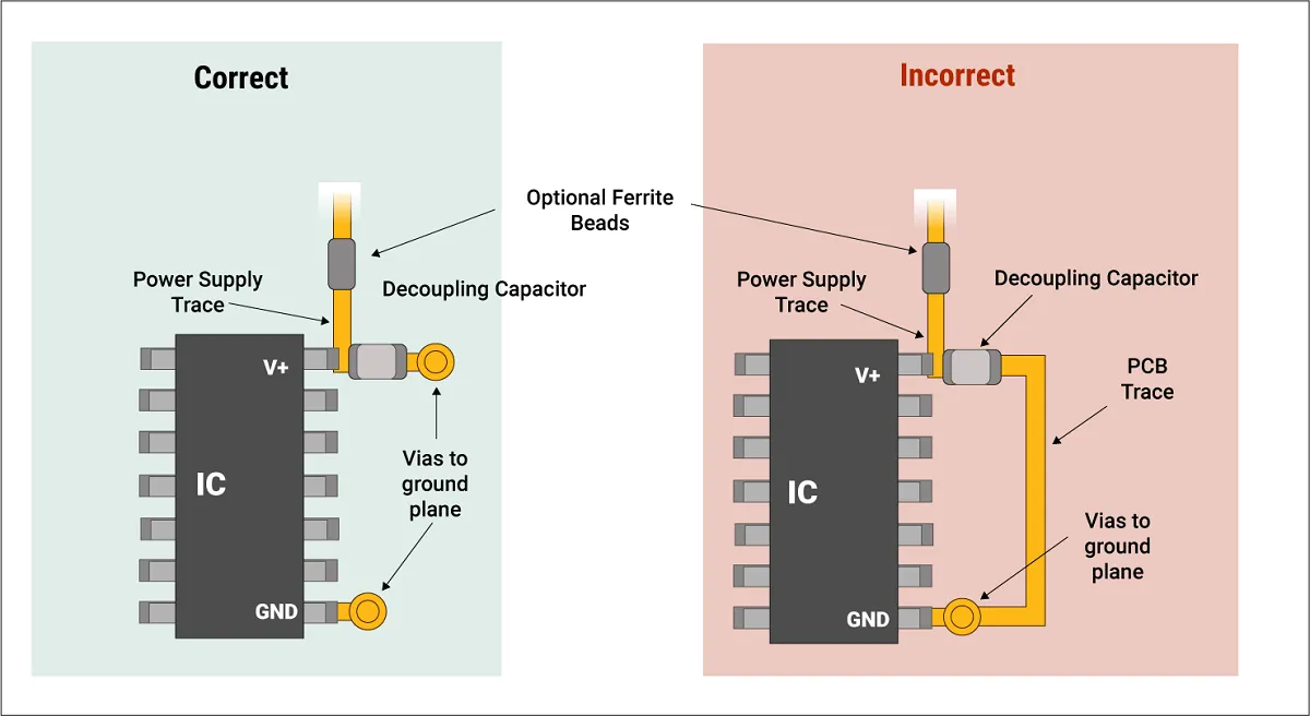
Bulk capacitors (typically 10-100µF or larger) stabilize the overall supply rail and handle lower-frequency energy storage and transients from the regulator. Decoupling capacitors (0.01-0.1µF range, placed very close to IC power pins) suppress high-frequency noise and provide fast local charge delivery.
A common manufacturing-observed failure occurs when designers use only one type or place them too far from pins, leading to increased effective series inductance (ESL) and impedance peaks. In multilayer boards, combine values strategically to achieve a flat PDN impedance profile across frequencies.
Proper placement minimizes loop areas and prevents voltage droops during switching events. In high-density designs, this directly impacts yield by reducing noise-induced errors during functional testing.
Via Placement and Power Pin Connection Best Practices
Multiple vias in parallel for power pins significantly reduce current density, inductance, and resistance compared to a single via. A lone via often creates bottlenecks that cause localized heating and voltage drops under load, issues frequently caught during DFM review or thermal validation.
Best practice recommends at least 2-4 vias per high-current pin, sized according to manufacturer capabilities and placed to minimize path length. In 4-layer and higher boards, connect directly to internal power planes where possible. This approach improves thermal dissipation and reliability in applications with varying loads.
Power Planes, Return Paths, and Loop Area Management
While power planes provide low-impedance distribution, they do not automatically resolve all problems. Component placement, short return paths (ideally adjacent ground planes), and controlled loop areas remain critical. Long return paths increase inductance and EMI susceptibility, leading to signal integrity issues even with solid planes.
In production, poor loop management can cause boards to fail EMC testing or exhibit crosstalk. Prioritize adjacent power-ground plane pairs in the stackup and use stitching vias judiciously.
Real Manufacturing Challenges in Multilayer Power Design
CAM engineers regularly encounter power-related DFM issues such as insufficient annular rings on high-current vias, trace width violations per IPC-2152, or plane splits that create unexpected return paths. These lead to fabrication defects like etching inconsistencies or plating problems in high-aspect-ratio vias.
Thermal management adds another layer: high current density causes copper heating, potentially resulting in delamination or warpage during reflow. For HDI or automotive boards, strict adherence to via strategies and symmetric stackups prevents these failures. Early simulation and manufacturer consultation during the design phase mitigate risks effectively.
FAQ
Q1: Why does my PCB reset under load even when powered on?
A1: This is often caused by inadequate power design — insufficient current capacity, poor decoupling, or high inductance from single vias rather than firmware issues.
Q2: How many vias should I use for power pins on a PCB?
A2: Multiple vias are recommended for power pins to reduce current density and inductance. A single via frequently creates voltage drops and instability under load.
Q3: Does adding a power plane solve all PCB power problems?
A3: No. While helpful, a power plane requires proper component placement, short return paths, and controlled loop areas to be effective. It is not a complete solution by itself.
Q4: What are common DFM issues with PCB power planes during manufacturing?
A4: Issues include inadequate clearance around plane splits, via thermal relief conflicts causing weak connections, and copper balancing problems leading to etch or plating variations. Consult your fabricator early for stackup-specific guidelines.
Q5: How do startup spikes affect power design in IoT devices?
A5: Inrush currents from capacitors and peripherals can exceed steady-state draw significantly. Without proper bulk capacitance and regulator sizing, this causes voltage sags that destabilize MCUs or sensors during boot sequences.
Board powers on. Then it resets under load.
You blame firmware.It's your power design.
1. Not knowing current requirements
You picked a regulator without checking the actual current.
MCU, sensors, LEDs, startup spikes, it all adds up.
If you don't know the numbers,you're designing blind.
2. No bulk and decoupling strategy
You added a few capacitors because the reference design had them.
But bulk caps and decoupling caps do different jobs.
Without a strategy, voltage drops are guaranteed.
3. Single via for power pins
One thin trace.
One via to the plane. Looks clean.
But current density and inductance don't care about clean.
4. Assuming one power plane fixes everything
"Just pour a plane. Problem solved."
No. Return paths, placement, and loop size still matter.
A plane is not magic.
Stable power is designed before routing begins.





