Introduction
Power supply printed circuit boards form the critical foundation for delivering stable voltage and current to electronic systems across industries like telecommunications, industrial controls, and consumer electronics. These PCBs endure high thermal loads, electromagnetic interference, and mechanical stresses that can lead to failures such as no output, erratic voltages, or complete shutdowns. Power supply PCB troubleshooting demands a systematic approach to minimize downtime and avoid cascading damage to connected devices. For electric engineers, diagnosing faults in power supply PCBs involves combining visual checks, electrical measurements, and component-level analysis to pinpoint root causes efficiently. This guide provides actionable steps for power supply PCB repair, focusing on prevalent issues like voltage drops and overheating. By following these methods, engineers can restore functionality while adhering to proven engineering practices.
Why Power Supply PCBs Fail and Why Troubleshooting Matters
Power supply PCBs integrate components like transformers, rectifiers, capacitors, regulators, and inductors in dense layouts optimized for efficiency and compactness. Failures often stem from thermal cycling, which causes material expansion and contraction, leading to cracked solder joints or delaminated layers. Electrical overloads exacerbate these problems, resulting in trace scorching or component burnout under sustained high currents. Environmental factors such as humidity accelerate electrolytic capacitor degradation, manifesting as leakage or capacitance loss that disrupts voltage regulation. Power supply PCB voltage issues frequently arise from these combined stressors, compromising output stability and risking downstream circuit damage.
Effective troubleshooting matters because power supplies operate continuously in mission-critical setups, where even brief outages incur significant costs. Engineers who master power supply PCB troubleshooting can isolate faults rapidly, extending board lifespan and enhancing system reliability. Neglecting systematic diagnosis often leads to unnecessary board replacements, inflating repair expenses. Moreover, understanding failure modes informs design improvements, such as wider power traces or better thermal vias, preventing recurrence. In high-volume production, quick fault diagnosis aligns with quality control goals, ensuring compliance with assembly standards. For deeper insights into maintaining stable output, see our guide on improving power integrity in power supply PCBs.
Common Causes of Power Supply PCB Problems
Overheating ranks among the top culprits in power supply PCB failures, often due to undersized traces carrying excessive current, which generates resistive heat and migrates copper. Components like switching transistors or diodes dissipate power as heat, and without adequate dissipation paths, temperatures exceed safe limits, causing insulation breakdown or solder reflow. Visual signs include browned laminate or charred pads, signaling immediate shutdown risks. Engineers should note that prolonged exposure warps the board, complicating further repairs.
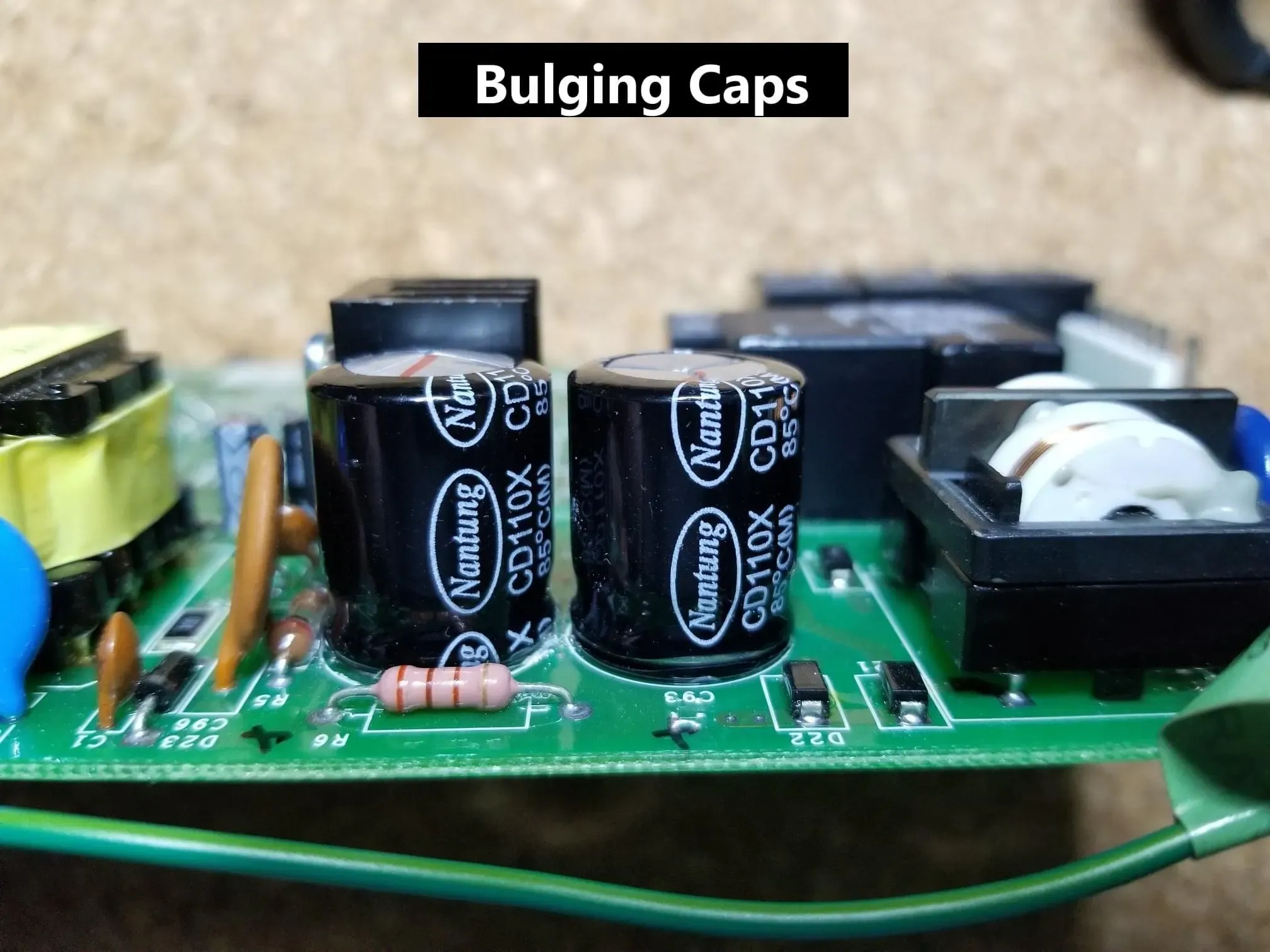
Capacitor failures, particularly in electrolytic types used for filtering, contribute to power supply PCB voltage issues through drying out or electrolyte evaporation over time. These manifest as increased equivalent series resistance, amplifying ripple voltage on DC outputs and starving regulators of stable input. Short-circuited capacitors create direct paths that blow fuses or stress upstream rectifiers. Bulging tops or crusty residues serve as telltale indicators during initial inspections.
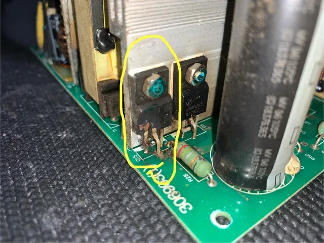
Solder joint defects from assembly processes lead to intermittent connectivity, where high-reliability joints crack under vibration or thermal shock. Poor wetting or insufficient fillet height, as defined in industry criteria, allows high-resistance paths that drop voltage under load. Diode or transistor failures often couple with these, presenting as open circuits after avalanche breakdown from voltage transients.
Layout-induced problems like ground loops introduce noise, coupling into sensitive feedback circuits and destabilizing regulation loops. Narrow power planes cause voltage sag during peak loads, mimicking regulator faults. Parasitic inductances in long traces provoke ringing, observable as voltage overshoots that damage semiconductors.
Step-by-Step Guide to Diagnosing Power Supply PCB Problems
Begin power supply PCB troubleshooting with a thorough visual inspection under magnification, checking for burnt traces, popped capacitors, or flux residues that bridge pads. Compare against a known-good board schematic to spot anomalies like missing components or mechanical damage from handling. Debris or corrosion on connectors often points to environmental ingress, requiring cleaning with isopropyl alcohol before proceeding.
Power off continuity tests using a multimeter isolate shorts or opens: probe power rails to ground for low resistance indicating bridges, and check diodes for forward bias. Verify fuse integrity and transformer windings for continuity without shorts. These steps reveal assembly flaws early, avoiding powered tests on hazardous boards.
Energize the board at reduced input voltage, monitoring current draw with a current-limited supply to prevent further damage. Measure DC voltages at key nodes: input rectifier output, filter caps, and regulator pins against expected values. Deviations signal specific zones, such as low rectifier output from failed bridge diodes.
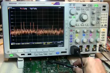
For dynamic analysis, employ an oscilloscope to capture ripple on output rails, where excessive AC content above 50 mV peak-to-peak suggests filter capacitor degradation. Probe switching node waveforms for abnormal duty cycles indicating control IC faults. Load testing with resistors simulates real conditions, exposing voltage droops from PDN weaknesses.
Thermal imaging identifies hot spots during operation, correlating elevated temperatures over 100 degrees Celsius with trace overloads or failing semiconductors. Cross-reference with airflow patterns to rule out cooling deficiencies.
Inspect solder joints per IPC-A-610 criteria, focusing on heel fillet formation and void absence for class 3 assemblies common in power supplies. Cracked joints appear dull or concave, confirming vibration-induced fatigue.
Practical Repair Techniques for Power Supply PCB Problems
Once diagnosed, power supply PCB repair starts with component replacement using hot air rework stations for SMD parts, ensuring pad cleanliness to prevent tombstoning. For through-hole electrolytics, desolder with braided wick, applying fresh flux for reliable new joints compliant with J-STD-001 requirements. Test replacements in-circuit before full power-up.
Address trace damage by jumper wires sized for current capacity, epoxied for strain relief, or copper foil overlays for wider paths. Recut scorched areas with precision knives, avoiding laminate delamination.
Regulator ICs demand careful pin lifting for substitution, verifying datasheet polarities to sidestep reverse damage. Feedback networks may need resistor tweaks for recalibration post-repair.
After fixes, perform burn-in testing under elevated temperature and load for several hours, monitoring stability. Final functional verification includes efficiency measurements and transient response.
Preventive measures include reinforcing high-stress joints with conformal coating and incorporating snubbers across switches. Design iterations should widen high-current paths per thermal rise calculations.
When replacing components or addressing assembly-related defects, consider our resources on solving plated through-hole problems.
Real-World Troubleshooting Insights
In one scenario, a power supply exhibited intermittent no-output under load, tracing to a cracked solder joint on the optocoupler per IPC-A-610 inspection. Reflow resolved it, but thermal cycling tests revealed layout vibration amplification. Engineers mitigated by adding mechanical standoffs.
Another case involved chronic voltage sags, diagnosed via scope as PDN inductance; adding bulk caps near loads stabilized rails. These examples underscore methodical progression from symptom to root cause.
Conclusion
Mastering power supply PCB troubleshooting equips electric engineers to tackle voltage issues, overheating, and connectivity faults with precision. Systematic visual, static, and dynamic tests pinpoint failures efficiently, enabling targeted repairs that extend board life. Adhering to standards ensures rework quality, while insights inform robust designs. Implement these practices to enhance reliability in power-critical applications, reducing failures and optimizing performance.
FAQs
Q1: What are the initial steps in power supply PCB troubleshooting?
A1: Start with visual inspection for burnt components, bulging capacitors, or poor solder joints. Disconnect power and perform continuity checks for shorts between rails and ground. Verify input fuse and transformer integrity using a multimeter. These non-invasive steps safely isolate obvious faults before powered testing, preventing further damage during diagnosis.
Q2: How do you diagnose power supply PCB voltage issues?
A2: Measure DC levels at rectifier output, filter capacitors, and regulator pins under no-load and full-load conditions. Use an oscilloscope to check ripple below 50 mV and absence of spikes. Voltage drops indicate trace resistance or capacitor ESR rise; compare against schematic expectations. Isolate by lifting suspect component pins for verification.
Q3: What causes overheating in power supply PCBs and how to repair it?
A3: Narrow traces, failing regulators, or blocked airflow generate excess heat, visible as discoloration. Repair by replacing damaged parts, widening traces with jumpers, and improving vias. Thermal imaging confirms fixes; add heat sinks for prevention. Follow rework guidelines to maintain integrity.
Q4: Can power supply PCB repair always restore full functionality?
A4: Most faults like capacitor or joint failures yield full recovery with proper diagnosis and replacement. However, multilayer delamination or extensive trace damage may require board scrap. Burn-in testing post-repair verifies stability, ensuring long-term reliability in operation.
References
IPC-A-610H — Acceptability of Electronic Assemblies. IPC, 2019
J-STD-001H — Requirements for Soldered Electrical and Electronic Assemblies. IPC, 2018
IPC-7711B/7721B — Rework, Modification and Repair of Electronic Assemblies. IPC, 2018


