Introduction
Power integrity in power supply PCBs forms the foundation for reliable operation in modern electronic systems. Engineers designing power supply boards face challenges like voltage fluctuations and electromagnetic interference that can degrade performance. Achieving strong power supply PCB power integrity ensures stable voltage delivery to sensitive loads, preventing issues such as signal distortion or component failure. This guide explores key strategies for power supply PCB voltage regulation, power supply PCB noise reduction, and optimal use of power supply PCB decoupling capacitors. By focusing on proven engineering practices, you can enhance overall system reliability and efficiency. Understanding these elements allows electric engineers to create robust designs that meet demanding application requirements.
What Is Power Integrity in Power Supply PCBs and Why It Matters
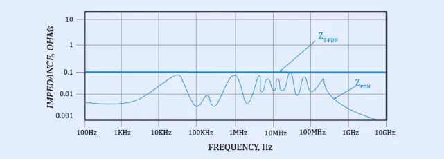
Power integrity refers to the ability of a power distribution network (PDN) in a PCB to deliver clean, stable power with minimal voltage drop or noise across the operational frequency range. In power supply PCBs, this involves managing the impedance profile from the voltage regulator module to the load points. Poor power integrity leads to voltage droop during transient events, causing timing violations in digital circuits or instability in analog sections. Noise coupling into signal lines can increase bit error rates or trigger electromagnetic compatibility failures. For electric engineers, prioritizing power supply PCB power integrity directly impacts product yield, thermal management, and compliance with performance specs. Ultimately, it determines whether a design passes validation testing and performs reliably in real-world conditions.
Core Technical Principles of Power Integrity
The PDN in a power supply PCB behaves as a distributed RLC network, where resistance from traces and vias, inductance from current paths, and capacitance from planes define the overall impedance. At low frequencies, plane capacitance dominates, providing a low-impedance path, but resonances occur where inductive and capacitive reactances align, peaking impedance and amplifying noise. Switching regulators introduce high-frequency ripple, while simultaneous switching noise from loads creates transient demands that challenge voltage stability. Target impedance budgeting helps engineers set maximum PDN impedance limits based on allowable voltage ripple and current draw. Accurate modeling requires considering skin effect, which increases effective resistance at higher frequencies, and dielectric losses in laminates. These principles guide layout decisions to maintain power supply PCB voltage regulation within tight tolerances.
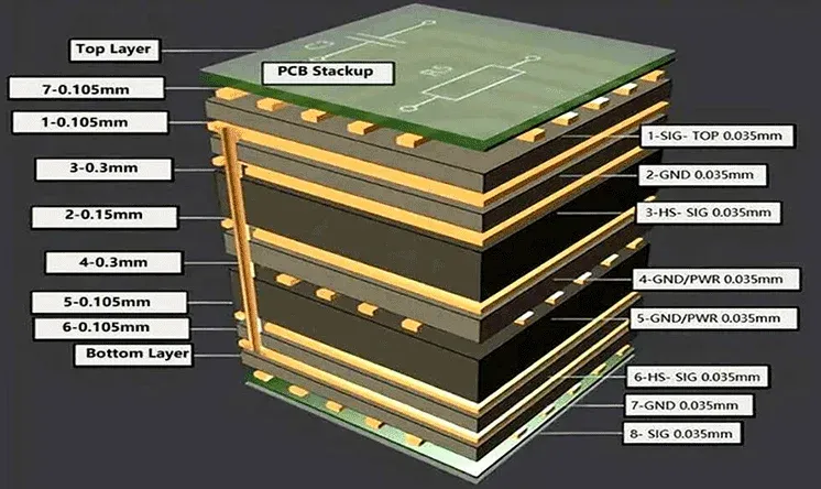
Voltage regulation in power supply PCBs relies on minimizing loop inductance in the feedback and output paths of regulators. Long traces or poor ground returns elevate inductance, slowing response to load steps and causing overshoot or undershoot. Parasitic inductance between power and ground planes forms a tank circuit, resonating at frequencies inversely proportional to the square root of LC values. Engineers must calculate these effects during the design phase to predict droop magnitudes. Stackup choices influence plane separation, directly affecting loop inductance per unit length. Adhering to guidelines in IPC-2221B ensures these parameters stay within acceptable bounds for reliable power supply PCB voltage regulation.
Noise in power supply PCBs arises from multiple sources, including clock harmonics, power switching edges, and crosstalk between adjacent nets. Ground bounce occurs when fast current changes through package leads induce voltage on ground references, coupling into other circuits. Return path discontinuities disrupt current flow, forcing noise to radiate or conduct through the board. Effective power supply PCB noise reduction demands continuous return planes to provide low-inductance paths for all currents. Fabricating boards with controlled impedance layers helps suppress broadband noise propagation. These mechanisms underscore the need for holistic PDN optimization from schematic to layout.
Best Practices for Enhancing Power Integrity
Start with layer stackup design to dedicate inner layers to solid power and ground planes, minimizing separation for low inductance. Avoid splitting planes under high-current paths, as splits force current to detour, increasing inductance and emissions. Use via stitching along plane edges to couple power and ground, reducing slot antenna effects that radiate noise. For multi-voltage domains, implement guard traces or moats with care to prevent coupling between sections. These foundational steps form the basis for robust power supply PCB power integrity.
Power supply PCB decoupling capacitors play a critical role in shunting high-frequency noise and supplying transient currents locally. Place multiple capacitors in parallel hierarchies: low-ESR ceramics for mid-frequencies near IC power pins, followed by bulk electrolytics for low frequencies farther out. Optimal spacing follows the rule of one capacitor per 1-2 cm along the load line, tuned to bypass expected noise spectra. Via-in-pad configurations minimize ESL, ensuring effective parasitics. Simulate placement to verify impedance flattening across the bandwidth. Proper implementation of power supply PCB decoupling capacitors can reduce PDN impedance by orders of magnitude at key frequencies.
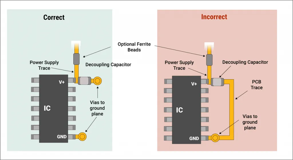
For power supply PCB voltage regulation, optimize regulator layout by minimizing the hot loop area encompassing input capacitors, inductor, and output capacitors. Position sense lines close to the load to compensate for trace drops accurately. Employ Kelvin connections for feedback to avoid noise pickup. In high-current designs, widen power traces and use multiple vias in parallel to lower resistance. Compliance with IPC-6012DS fabrication specs ensures planar uniformity, preventing hotspots that degrade regulation. These practices stabilize output voltage under varying loads.
Power supply PCB noise reduction benefits from strategic filtering and shielding. Integrate ferrite beads in series with power inputs to attenuate high-frequency components without affecting DC. Common-mode chokes on input lines suppress differential and common-mode noise effectively. Maintain consistent ground topology, preferring a single solid plane over split or meshed grounds for broadband performance. Controlled trace routing away from sensitive analog sections reduces crosstalk. Post-layout simulations validate these measures before prototyping.
Advanced techniques include embedded passives within the board for distributed decoupling, reducing discrete component count and parasitics. Optimize board thickness and material properties to control propagation delays in PDN resonances. During verification, time-domain reflectometry measures PDN discontinuities accurately. Fabricators following J-STD-001G assembly standards ensure reliable capacitor soldering joints, preserving decoupling effectiveness. Integrating these methods yields superior power supply PCB power integrity.
Common Troubleshooting Scenarios
Engineers often encounter excessive ripple traced to insufficient bulk capacitance or poor input filtering. Measure PDN impedance with vector network analyzers to identify resonance peaks, then add targeted capacitors to dampen them. Voltage droop during load steps signals high loop inductance; shorten paths and add stitching vias. Noise floor elevation points to ground discontinuities; review return current paths in simulations. Prototype testing with oscilloscopes under worst-case loads reveals real-world behaviors. Systematic application of these diagnostics resolves most power supply PCB issues efficiently.
Conclusion
Improving power integrity in power supply PCBs demands a systematic approach from PDN modeling to layout optimization. Key strategies like solid planes, strategic decoupling, and minimal loop areas ensure stable voltage regulation and low noise. Electric engineers benefit from simulating early and verifying prototypes rigorously. Implementing power supply PCB decoupling capacitors effectively bridges simulation to reality. These practices not only enhance performance but also reduce design iterations. Prioritizing power supply PCB power integrity leads to reliable, high-yield products ready for production.
FAQs
Q1: How can engineers improve power supply PCB power integrity during the design phase?
A1: Focus on low-impedance PDN design with dedicated power and ground planes, minimal splits, and via stitching. Simulate target impedance profiles to guide stackup choices. Place decoupling capacitors hierarchically near loads to handle transients. Verify layouts against engineering models before fabrication. This structured approach ensures stable power delivery across frequencies.
Q2: What role do power supply PCB decoupling capacitors play in voltage regulation?
A2: Decoupling capacitors provide local charge reservoirs, compensating for inductive voltage drops during fast load changes. Parallel combinations cover broad frequency ranges, flattening PDN impedance. Proper placement reduces ESL and ESR effects. Engineers select values based on noise spectra and current demands. Effective decoupling maintains tight voltage regulation tolerances.
Q3: What are effective methods for power supply PCB noise reduction?
A3: Use continuous ground planes for low-inductance returns and ferrite filters to block high-frequency ingress. Avoid plane splits and ensure stitching vias couple sections. Route traces with controlled impedance to minimize crosstalk. Post-layout EMI scans identify issues early. These techniques suppress noise coupling effectively.
Q4: Why is stackup design critical for power supply PCB power integrity?
A4: Stackup determines plane capacitance and separation, directly impacting PDN inductance and resonance frequencies. Thin dielectrics between power-ground pairs lower impedance. Symmetric builds prevent warpage affecting connections. Optimal sequencing isolates noisy sections. Proper stackup forms the backbone of reliable power integrity.
References
IPC-2221B - Generic Standard on Printed Board Design. IPC, 2009
IPC-6012DS - Qualification and Performance Specification for Double-Sided Flexible Printed Boards. IPC, 2015
J-STD-001G - Requirements for Soldered Electrical and Electronic Assemblies. IPC, 2011


