 00:59
00:59
PCB Routing
PCB routing forms a critical phase in the design of printed circuit boards, where engineers strategically connect components through conductive traces to ensure optimal signal integrity, power distribution, and overall functionality. This tag encompasses a wide array of resources dedicated to mastering PCB routing techniques, from basic trace layout principles to advanced strategies for high-speed and high-density boards. For professionals, hobbyists, and students searching for guidance on PCB routing, these articles provide essential knowledge to avoid common pitfalls such as crosstalk, electromagnetic interference, and thermal issues that can compromise circuit performance. Understanding PCB routing begins with selecting appropriate trace widths, spacing, and layer configurations based on current requirements and signal frequencies. Practical applications include designing efficient multilayer boards for complex electronics like smartphones, automotive systems, and IoT devices, where precise routing minimizes noise and enhances reliability. Best practices highlighted here emphasize tools like auto-routers in CAD software, manual fine-tuning for critical paths, and adherence to standards such as IPC-2221 for manufacturability. Readers can gain actionable insights into differential pair routing for high-speed data transmission, via optimization to reduce impedance discontinuities, and strategies for routing in constrained spaces without sacrificing board integrity. By exploring the content under this tag, you'll discover step-by-step tutorials, case studies, and expert tips that address real-world challenges, helping you refine your designs for better efficiency and cost-effectiveness. Whether you're troubleshooting a prototype or scaling up for production, these resources equip you with the tools to achieve robust, error-free PCB layouts that meet industry demands.
Video Guide

Technical Articles

How AI Can Assist Multilayer PCB Routing and Design

PCB Design Guidelines: Key Routing and Layout Considerations
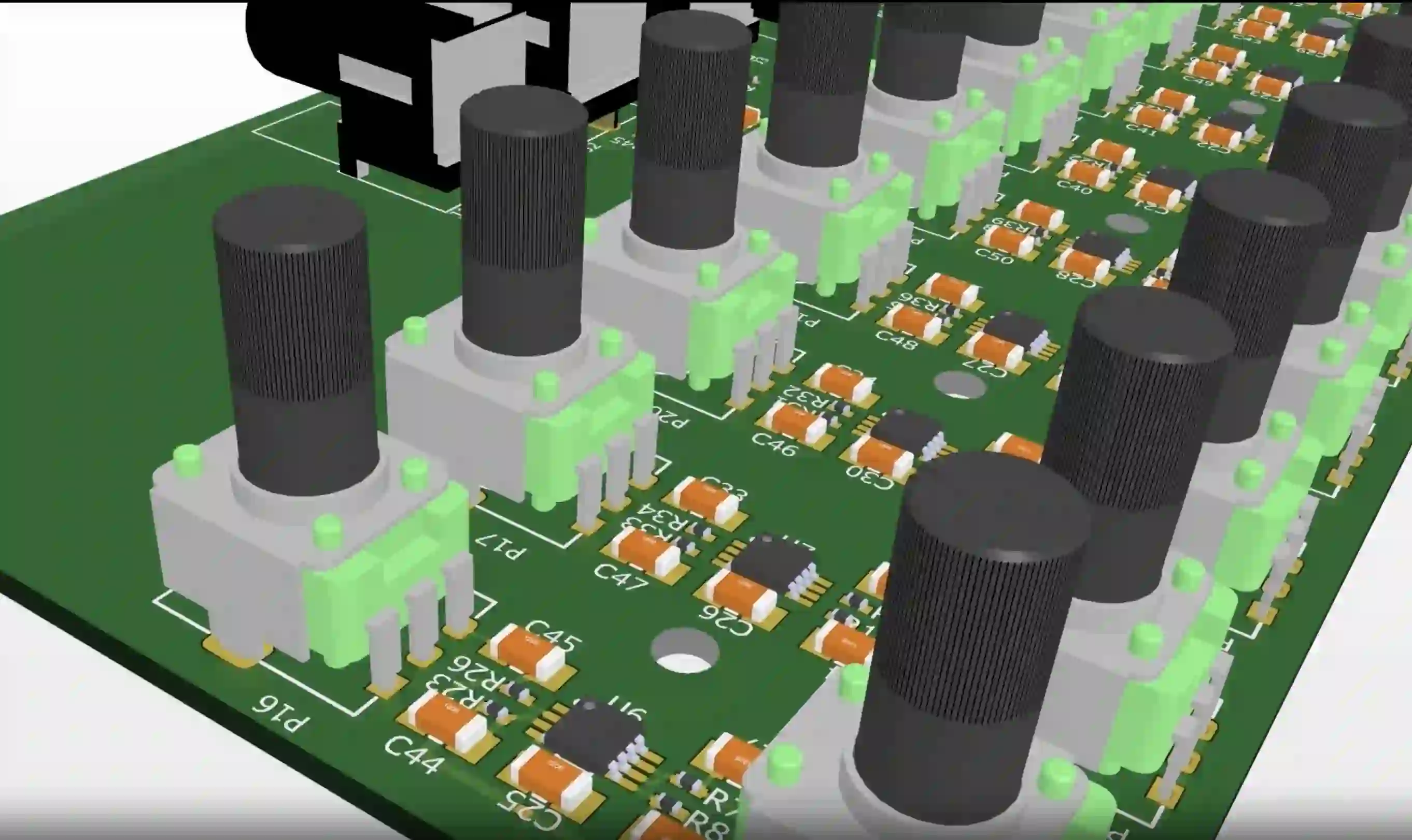
Mixed Signal PCB Routing Strategies: Minimizing Interference and Maximizing Performance
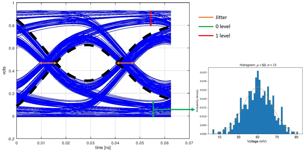
Routing Techniques for High Speed Digital PCBs: Minimizing Signal Degradation
Multilayer PCB Design: A Beginner’s Guide to Routing
Impedance Control: Optimizing Signal Transmission in Embedded Component PCBs
Through Hole Via Placement Strategies for Optimal Signal Routing
PCB Press-Fit Hole Design Rules for Heavy Copper Boards
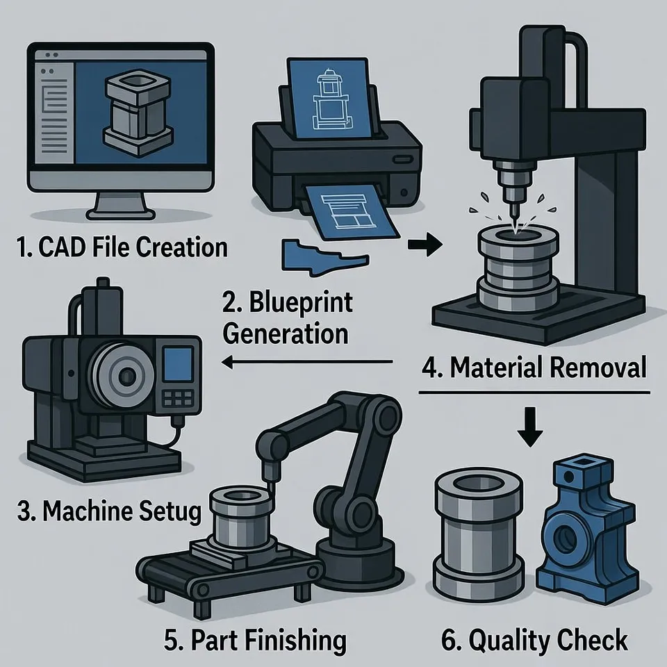
CNC Machining Process Explained: From CAD File to Finished Part
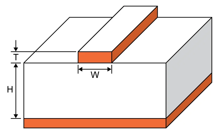
Advanced RF PCB Routing Techniques: Mastering Microstrips and Striplines
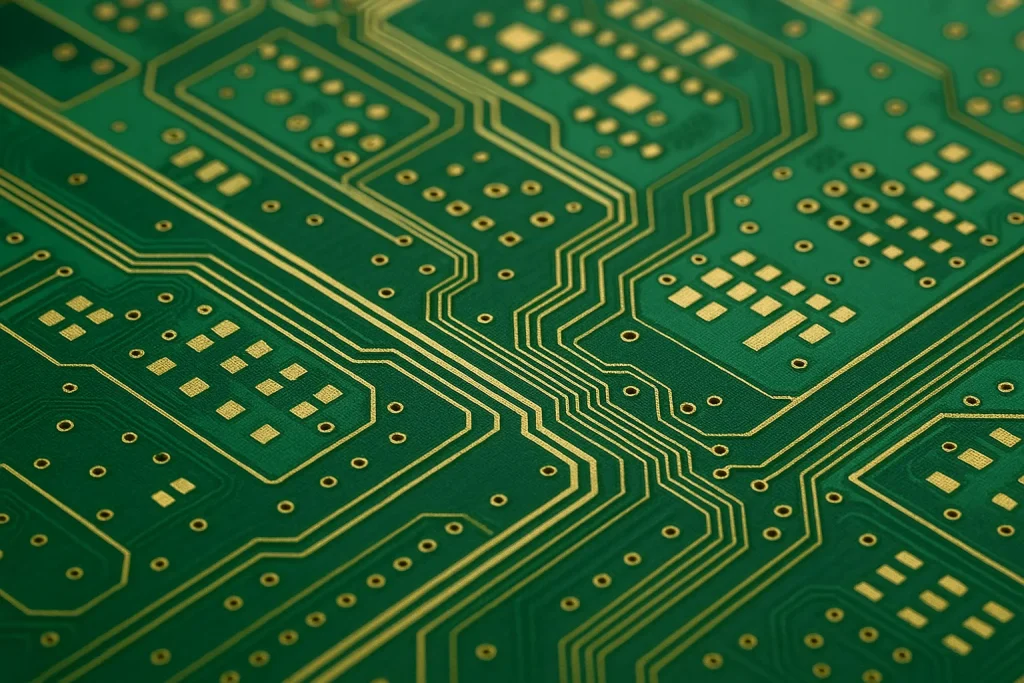
High Frequency PCB Routing Techniques: Minimizing Signal Loss and Interference
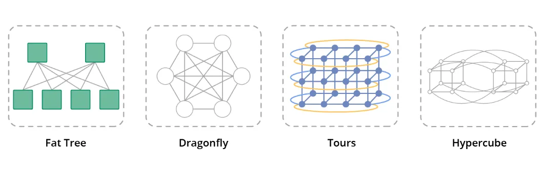
InfiniBand Networks: HDR and IB Technology Overview
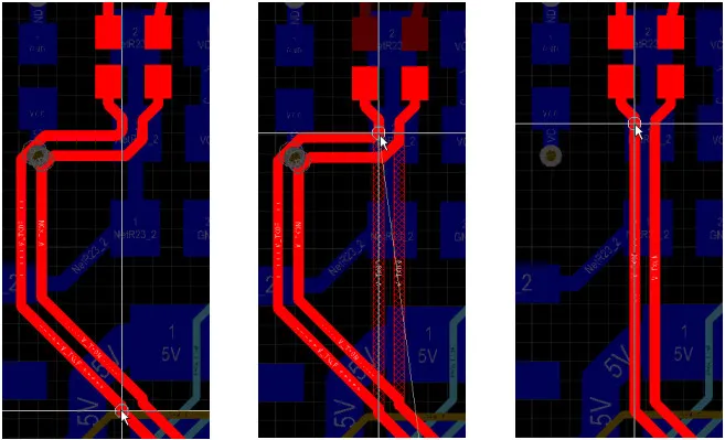
Maximizing Efficiency: Effective Strategies for PCB Routing
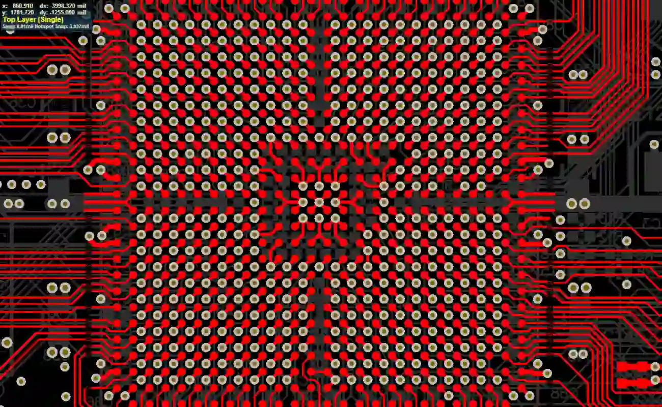
Signal Integrity Showdown: Via in Pad vs. Dog Bone Routing

High Speed PCB Routing: Achieving Impedance Control for Signal Integrity
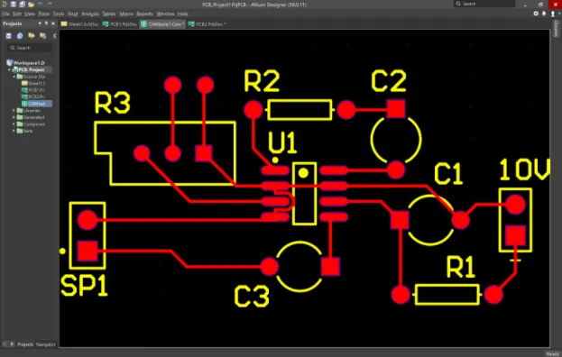
PCB Routing Techniques: A Comprehensive Guide to Efficient Trace Layout
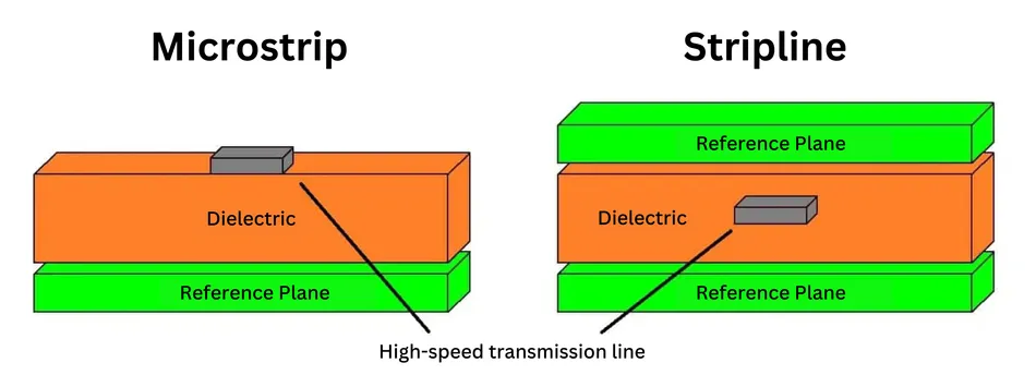
Advanced Routing Techniques for High Frequency PCB Designs
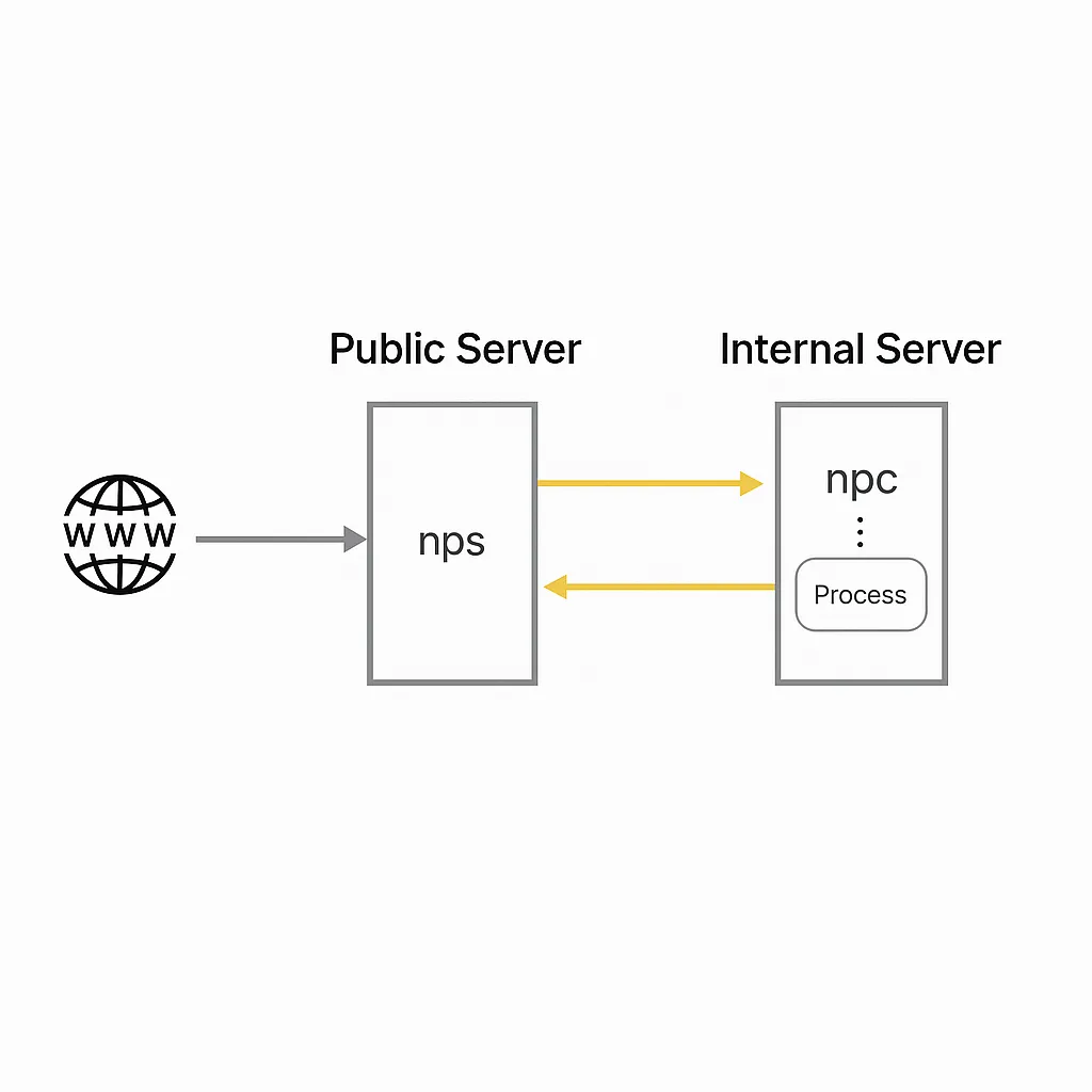
Common NAT Traversal Tools: Principles and Usage
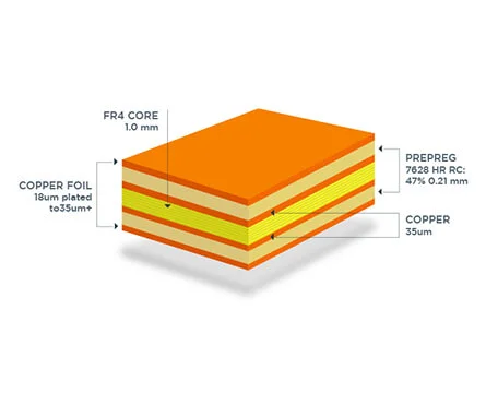
Optimizing Signal Integrity in Rigid PCB Design: Techniques and Best Practices