Introduction
High-speed PCB routing demands precise control over signal paths to maintain integrity in modern electronics. As data rates climb into gigabits per second, signals behave as transmission lines where mismatches lead to reflections and degradation. Impedance matching becomes essential to prevent these issues, ensuring clean signal transmission from source to receiver. Controlled impedance routing involves designing traces with specific characteristic impedances tailored to the application’s needs. This approach minimizes losses and crosstalk, critical for performance in telecommunications, computing, and automotive systems. Engineers must integrate these principles early in the design process to avoid costly revisions.

Understanding Transmission Line Impedance in PCBs
Transmission line impedance defines the opposition to signal propagation along a PCB trace, determined by geometry and materials. Trace impedance arises from the interaction between the conductor, dielectric, and reference planes, modeled as microstrip or stripline structures. In microstrip lines, the trace sits on top of the dielectric with air above, while striplines are embedded between planes. The characteristic impedance Z0 follows equations influenced by trace width, thickness, dielectric height, and dielectric constant. Engineers calculate these using field solvers or approximations from standards like IPC-2141A. Proper control ensures signals arrive undistorted, preserving eye diagrams and bit error rates.
The dielectric constant, often denoted as Er, plays a pivotal role in transmission line impedance. Materials with higher Er confine fields more tightly, lowering impedance for given dimensions. Common FR-4 resins exhibit Er around 4.0 to 4.5, varying with frequency and glass content. Variations in Er across the board can introduce inconsistencies, complicating controlled impedance routing. Manufacturers test coupons to verify Er uniformity before lamination. Selecting stable dielectrics supports reliable impedance matching across production runs.
Suggested Reading: How to Calculate Impedance of Transmission Lines for High-speed PCB Designs
Factors Influencing Trace Impedance
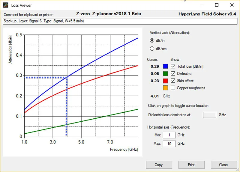
Several geometric and material factors dictate trace impedance in high-speed designs. Trace width directly impacts impedance: wider traces reduce Z0 due to increased capacitance. Copper thickness, typically 1 oz or 2 oz per square foot, affects both resistance and inductance. Dielectric thickness between trace and reference plane inversely influences capacitance, thus Z0. Surface roughness on copper adds skin effect losses at high frequencies, subtly altering effective impedance. Engineers balance these during stackup planning to achieve target values like 50 ohms single-ended or 100 ohms differential.
Impedance discontinuity occurs when abrupt changes in trace geometry or surroundings disrupt uniform Z0. Vias, bends, or plane splits create reflections proportional to the mismatch. These discontinuities generate ringing or overshoot, degrading signal integrity. Length-matched routing mitigates phase skew in differential pairs. Adhering to design guidelines from IPC-2221C helps minimize such issues through consistent spacing and via strategies. Simulations validate layouts before fabrication.
Microstrip vs Stripline for High-Speed Routing
| Configuration | Structure | Impedance Control | Crosstalk / EMI | Routing Density | Best Applications | Limitations |
|---|---|---|---|---|---|---|
| Microstrip | Trace on outer layer, air above, ground below | Good (easier to fabricate) | Higher (exposed fields) | High on surface | Cost-sensitive, accessible layers | More susceptible to external interference |
| Stripline | Trace embedded between two ground planes | Excellent (tight control) | Lower (shielded) | Lower (inner layers) | High-speed, low-noise, RF-critical nets | Harder to access, more layers needed |
Stripline generally offers superior impedance control and noise immunity for critical high-speed signals, while microstrip is more practical for cost-sensitive or prototype designs. Many boards use a hybrid approach: stripline for inner high-speed layers and microstrip for outer routing.
Principles of Controlled Impedance Routing
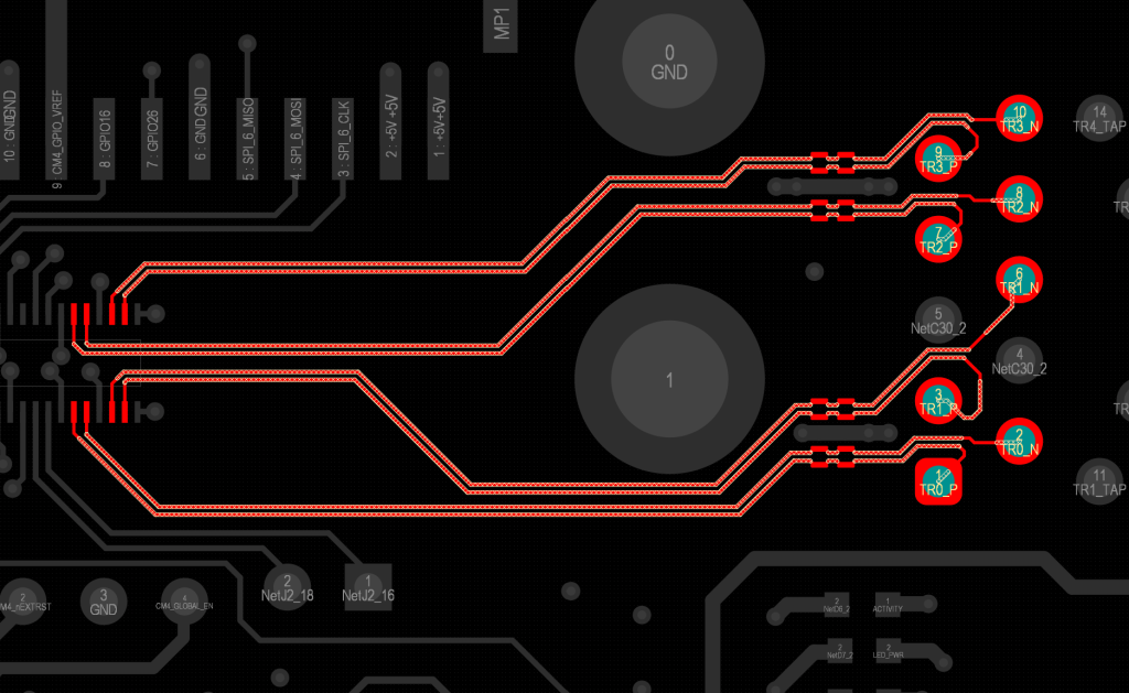
Controlled impedance routing starts with stackup definition, specifying layer materials and thicknesses for target Z0. Symmetric stackups with paired power-ground planes provide stable references. For single-ended signals, 50 ohms is common; differential pairs target 90-120 ohms depending on protocol. Routing tools enforce widths and gaps during placement. Length tuning ensures pairs arrive simultaneously, avoiding common-mode noise. Ground vias stitch planes near traces to contain return currents.
Differential routing demands tight coupling between traces, with constant spacing and no vias in one leg without the other. Edge-coupled pairs on outer layers suit microstrip, while broadside in inner layers offer tighter control. Avoid 90-degree bends; use 45-degree or curved paths to reduce radiation. Plane splits require stitching capacitors or vias to maintain low-inductance returns. Post-layout extraction confirms impedance profiles match specs. These practices align with IPC-2141A for high-speed performance.
Maintaining consistent reference planes prevents impedance discontinuities. Solid planes under signals provide broad return paths, minimizing inductance. Partial splits for power distribution need careful bridging. In dense boards, back-drilling vias shortens stubs that cause resonances. Fabricators provide test coupons for TDR verification, measuring Z0 along traces. Iterative design refines routing for optimal signal integrity.
Suggested Reading: Unlocking Signal Integrity: A Deep Dive into PCB Impedance Control
Best Practices for Achieving Impedance Matching
Begin with accurate stackup models incorporating real material properties. Collaborate with fabricators early for Er and loss tangent data. Use 3D field solvers for precise calculations beyond 2D approximations. Target tolerances like +/-10% for most designs, tighter for ultra-high speeds. Route critical nets first, reserving inner layers for high-speed signals.
Minimize vias through direct connections or blind/buried types. For unavoidable vias, optimize stub length below signal bandwidth. Fanouts from BGA packages require impedance-controlled escapes. Decoupling capacitors near ICs stabilize supplies, reducing noise coupling. Thermal management avoids hot spots altering Er. Final DRC checks flag violations. Engineers working on mixed-signal boards should also review our article on Optimizing Industrial Sensor PCB Layout for Signal Integrity and Noise Reduction for practical analog-digital routing considerations.
In production, specify impedance coupons on panels for verification. TDR or VNA testing confirms compliance before assembly. Adjust etch factors if needed for fine features. Documentation includes stackup drawings and target Z0. These steps ensure robust impedance matching.
Simulation and Verification Workflows
Modern high-speed routing relies on integrated simulation workflows. Pre-layout stackup analysis determines feasible trace geometries for target Z0. Post-layout 2D/3D field solvers extract S-parameters, eye diagrams, and crosstalk. Full-channel simulations include driver, transmission line, vias, and receiver models.
Verification combines TDR for impedance discontinuities, VNA for frequency-domain performance, and time-domain measurements on prototypes. Thermal-electrical co-simulation predicts material property shifts under operating conditions. Correlating simulation results with lab measurements builds confidence and reduces prototype iterations.
Troubleshooting Common Impedance Issues
Engineers often encounter reflections from poor via transitions. Analyze eye diagrams to quantify degradation. Shorten stubs or use back-drilling remedies. Crosstalk arises from inadequate spacing; increase gaps or shield with ground traces. Simulations predict coupling levels.
Dielectric variations cause Z0 wander. Use low-loss materials for GHz signals. Manufacturing tolerances on width and height demand margins. Post-fab testing identifies outliers. Rework focuses on critical nets. Systematic verification upholds signal integrity.
Real-World Case Studies and 2026 Trends
In a 112 Gbps SerDes design, improper via stub management caused a 6 dB notch at the Nyquist frequency. Implementing backdrilling and optimized via transitions restored a clean eye opening and enabled full data rate.
A high-density computing board reduced crosstalk by 18 dB by switching critical nets to stripline with dense stitching vias. In 2026, trends include wider adoption of low-loss, ultra-flat materials for mmWave, AI-assisted routing optimization for impedance and crosstalk, and increased use of embedded components to shorten high-speed paths. Hybrid microstrip/stripline stackups and advanced backdrilling techniques will become standard for next-generation designs.
Conclusion
High-speed PCB routing hinges on meticulous impedance control to safeguard signal integrity. Mastering transmission line impedance, influenced by dielectric constant and geometry, enables precise controlled impedance routing. Avoiding impedance discontinuities through best practices like length matching and plane management yields reliable designs. Standards such as IPC-2141A and IPC-2221C provide foundational guidance. Implementing these principles empowers engineers to deliver high-performance boards. Future designs will demand even tighter tolerances as speeds rise.
FAQs
Q1: What is trace impedance and why is it critical for high-speed PCBs?
A1: Trace impedance is the characteristic impedance of a PCB conductor acting as a transmission line, determined by width, thickness, dielectric constant, and reference plane distance. In high-speed designs, mismatches cause reflections, leading to signal distortion, overshoot, and bit errors. Controlled impedance routing maintains uniform Z0, ensuring impedance matching for clean propagation. Engineers target 50 ohms single-ended or 100 ohms differential per protocol requirements. Verification via TDR confirms compliance, preventing field failures.
Q2: How does the dielectric constant affect transmission line impedance?
A2: The dielectric constant (Er) measures a material’s ability to store electrical energy, directly impacting transmission line impedance. Higher Er increases capacitance, lowering Z0 for fixed dimensions. In PCBs, core and prepreg Er values around 3.5-4.5 influence stackup choices. Frequency-dependent Er variations add losses at high speeds. Designers select low, stable Er materials for controlled impedance routing. Simulations account for effective Er in multilayer boards.
Q3: What causes impedance discontinuity in PCB routing and how to mitigate it?
A3: Impedance discontinuity arises from geometry changes like vias, bends, pads, or plane gaps, creating reflections that degrade signal integrity. Vias introduce stubs acting as resonators; plane splits raise return path inductance. Mitigation includes back-drilling vias, stitching capacitors across splits, and smooth 45-degree bends. Length-matched controlled impedance routing preserves pairs. Pre-layout simulations and fab coupons verify uniformity. Adhering to design rules minimizes these effects.
Q4: Why is controlled impedance routing essential for impedance matching?
A4: Controlled impedance routing designs traces to specific Z0 values, ensuring impedance matching between driver, line, and receiver. Without it, reflections accumulate, closing eye openings in high-speed signals. Factors like trace width and dielectric constant are tuned precisely. Differential pairs require symmetric geometries for balance. This practice supports gigabit rates in serdes and DDR interfaces. Post-route analysis confirms targets within tolerance.
References
IPC-2141A - Design Guide for High-Speed Controlled Impedance Circuit Boards. IPC, 2004
IPC-2221C - Generic Standard on Printed Board Design. IPC, 2023


