Introduction
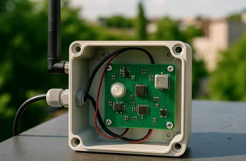
Industrial sensors play a critical role in monitoring processes across manufacturing, automation, and environmental control systems. These devices convert physical phenomena like temperature, pressure, or vibration into electrical signals that must remain accurate despite electromagnetic interference and layout-induced distortions. Optimizing sensor PCB layout directly impacts signal integrity PCB performance by preserving waveform fidelity and minimizing noise. Poor layout choices can amplify noise, leading to false readings or system failures in high-stakes environments. This article explores proven strategies for sensor PCB layout, focusing on grounding techniques PCB, shielding PCB, and differential signaling PCB approaches. Engineers can apply these methods to enhance reliability and meet demanding performance specifications.
Why Signal Integrity and Noise Reduction Matter in Sensor PCB Layout
Signal integrity PCB refers to maintaining the electrical quality of signals from source to receiver, crucial for sensors where microvolt-level precision determines output validity. In industrial settings, sensors often operate amid motors, power supplies, and RF sources that introduce noise through capacitive or inductive coupling. Noise reduction PCB techniques prevent degradation from crosstalk, ground bounce, or radiated emissions, ensuring compliance with functional requirements. Layout flaws, such as improper trace routing or inadequate ground returns, exacerbate these issues, potentially violating system margins. For electric engineers, prioritizing sensor PCB layout during design phases reduces debugging time and iteration costs. Ultimately, robust layouts support scalable production while upholding data trustworthiness.
Industrial standards like IPC-2221B emphasize controlled impedance and minimized discontinuities in high-speed or analog designs. Neglecting these can result in signal reflections or attenuation, particularly for low-level sensor outputs. Engineers must balance board size constraints with isolation needs to avoid compounding errors in feedback loops.
Fundamental Principles of Signal Integrity in Sensor PCBs
Signal integrity in sensor PCB layout hinges on controlled impedance matching across traces, vias, and terminations to prevent reflections. Transmission line theory dictates that traces longer than one-sixth of the signal rise time behave as lines requiring characteristic impedance control, typically 50 or 100 ohms for sensor applications. Return path integrity ensures low-inductance loops, as current flows in both signal and ground conductors equally. Discontinuities like stubs or unmatched lengths introduce ringing or overshoot, degrading edge rates. Engineers calculate stackup parameters to achieve uniform dielectric heights and plane spacing for consistent performance.
Via optimization minimizes parasitic inductance; blind or buried vias reduce stub effects compared to through-hole types. Component placement influences coupling; grouping sensors with their amplifiers shortens critical paths. Pre-layout simulations verify these principles before fabrication.
Crosstalk arises from mutual inductance or capacitance between adjacent traces, proportional to coupling length and inversely to separation. Aggressive bends or parallel runs amplify this, necessitating length staggering or ground shielding between lines.
Suggested Reading: Designing High Reliability Industrial Sensor PCBs for Harsh Environments
Common Noise Sources and Their Impact on Sensor PCBs
Noise in sensor PCB layout stems from multiple origins, including power supply ripple coupling into analog grounds and digital switching transients. Electromagnetic interference from external fields induces voltages via loop antennas formed by poor routing. Ground bounce occurs when multiple ICs share a ground pin, causing voltage fluctuations during simultaneous switching. Self-induced noise from high di/dt in power traces affects nearby sensors through magnetic fields. Understanding these mechanisms allows targeted mitigation in the layout phase.
Thermal noise and shot noise are inherent but layout-amplified by high-impedance paths. Radiated emissions couple back as susceptibility, closing the loop on system-level issues.
Grounding Techniques PCB for Optimal Noise Reduction
Grounding techniques PCB form the backbone of noise reduction PCB strategies by providing low-impedance return paths and equipotential references. A solid ground plane under analog sections minimizes loop areas, reducing inductive pickup. Single-point grounding suits low-frequency sensors to avoid ground loops, while multi-point schemes benefit high-frequency signals with plane capacitance bypassing. Star grounding converges returns at one node for DC sensors, preventing current sharing issues. Partitioning analog and digital grounds with a single bridge connection blocks digital noise ingress.
IPC-6012E specifies performance criteria for board-level integrity, indirectly supporting clean grounding through surface finish and plating requirements. Engineers route bridges narrow to limit high-frequency coupling while sizing for DC currents. Kelvin connections for precision sensors use separate sense traces to avoid IR drops. For comprehensive material and environmental considerations that complement these grounding strategies, see our guide on Designing High Reliability Industrial Sensor PCBs for Harsh Environments.
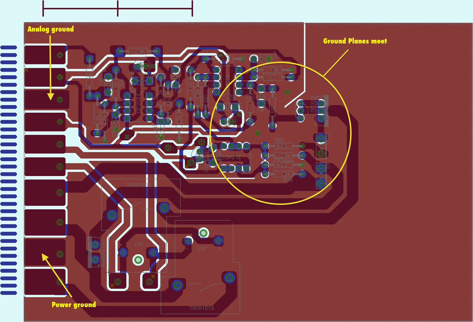
Guard traces around sensitive nets float or tie to analog ground, shunting stray fields. Verification involves probing ground impedance across frequencies.
Shielding PCB Methods to Combat EMI
Shielding PCB employs enclosures, cans, or on-board techniques to attenuate electromagnetic fields reaching sensor nodes. Copper pours surrounding traces act as Faraday cages when grounded, reflecting or absorbing waves based on skin depth. Via fencing around shielded areas stitches planes together, forming a continuous barrier below cutoff frequencies. Keep-out zones prevent overlapping fields between noisy and quiet sections. For compact boards, embedded shielding layers in stackups provide broadband protection.
Guard rings encircle low-level amplifiers, connected to ground via capacitors for AC shielding. These methods scale with frequency; low-frequency magnetic shielding requires mu-metal but PCB limits to layout isolation.
Differential Signaling PCB for Enhanced Signal Integrity
Differential signaling PCB transmits signals as balanced pairs, rejecting common-mode noise through subtraction at receivers. Ideal for thermocouples or strain gauges, this approach doubles noise immunity versus single-ended lines. Maintain equal lengths and symmetric routing to preserve balance, using length-matching tools during placement. Impedance control targets 100 ohms differential, with intra-pair spacing tighter than edge-to-edge. Crossovers introduce imbalance, so route pairs orthogonally to aggressors.
Twisted pair emulation on PCB uses serpentine meanders for length tuning without phase skew. Receivers with high CMRR amplify the difference while nulling offsets.
Suggested Reading: Optimizing Single Sided PCB Layout for Minimal Noise
Best Practices for Sensor PCB Layout Optimization
Start with stackup design favoring four or more layers for dedicated planes, ensuring 1:1 trace-to-plane spacing ratios. Place sensors peripherally to shorten external connections, grouping with local decoupling. Route analog signals first, innermost layers away from edges. Minimize vias on critical nets by fanning out components optimally. Power distribution uses wide polygons with decap stitching. When working with high-precision analog sensors, also review our article on high reliability industrial sensor PCBs for harsh environments for integrated thermal and vibration layout tips.
Filter ingress at connectors with pi-networks of ferrites and capacitors. Post-layout reviews check for 3W rule spacing between signal and power. Fabrication tolerances per J-STD-020E influence impedance, so specify tight controls.
Simulation and Verification Workflows
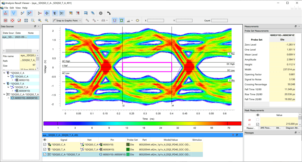
Modern workflows integrate pre-layout simulation for stackup and PDN optimization, followed by post-layout full-board analysis for signal integrity, crosstalk, and EMI. Tools model transmission lines, via effects, and differential pairs to predict eye diagrams, jitter, and noise margins.
Verification includes TDR for impedance discontinuities, VNA for S-parameters, and near-field probing for emissions/susceptibility. Correlate simulation results with prototype measurements under realistic industrial conditions (including temperature and vibration) to close the design loop and confirm performance before production.
Troubleshooting Common Layout Pitfalls
Common issues include ringing from unmatched impedances (diagnosed with TDR), crosstalk appearing as glitches on adjacent traces (solved by increased spacing or shielding), and 50/60 Hz hum from ground loops (resolved by proper partitioning or optical isolation).
Ground bounce during digital switching can shift analog references—mitigate with dedicated planes and decoupling. Simulate design iterations early and compare models against physical prototypes to identify discrepancies quickly. Systematic troubleshooting, guided by standards and measurement tools, minimizes respins.
DFM and Production Considerations for Reliable Sensor PCBs
DFM for sensor PCBs emphasizes fabrication-friendly geometries, generous tolerances on non-critical features, and clear documentation of analog zones and keep-out areas. Specify controlled impedance requirements and tight dielectric controls in fabrication notes.
Panelization should support uniform plating and etching for consistent resistor or trace values. Choose surface finishes (e.g., ENIG) that maintain low contact resistance for precision analog sections. Collaborate with manufacturers experienced in mixed-signal boards to ensure repeatability and high yields in production.
Conclusion
Optimizing sensor PCB layout demands integrated attention to signal integrity PCB, noise reduction PCB, grounding techniques PCB, shielding PCB, and differential signaling PCB. These strategies mitigate industrial noise challenges, ensuring precise sensor performance. Logical application of principles like plane partitioning and balanced routing yields robust designs. Adhering to standards enhances reproducibility. Electric engineers benefit from proactive layout planning, reducing field failures and supporting system reliability.
FAQs
Q1: What are the most effective grounding techniques PCB for analog sensors?
A1: Grounding techniques PCB prioritize split planes with a single bridge to isolate analog from digital noise. Solid ground under sensors minimizes inductive loops, while star points suit low-frequency returns. Guard traces shunt fields, and Kelvin sensing avoids drops. This setup per design guidelines preserves microvolt accuracy in noisy environments.
Q2: How does shielding PCB improve signal integrity PCB in industrial applications?
A2: Shielding PCB uses via-fenced pours and guard rings to attenuate EMI coupling into sensor traces. Grounded enclosures reflect fields, with skin effect aiding high frequencies. Placement away from board edges maximizes effectiveness. Combined with plane stitching, it boosts margins for signal integrity PCB without added components.
Q3: Why choose differential signaling PCB for noise reduction PCB?
A3: Differential signaling PCB rejects common-mode noise via balanced pairs, ideal for EMI-heavy industrial sensors. Symmetric routing maintains CMRR, doubling immunity over single-ended. Length matching prevents skew, supporting high-precision outputs. This enhances noise reduction PCB in layouts with limited isolation space.
Q4: What role does stackup play in sensor PCB layout?
A4: Stackup defines impedance and isolation in sensor PCB layout, with planes sandwiching signals for return paths. Symmetric builds control warpage, ensuring via reliability. Optimal dielectric thicknesses hit target Z0. Poor stackups amplify crosstalk, undermining noise efforts.
References
IPC-2221B — Generic Standard on Printed Board Design. IPC, 2009
IPC-6012E — Qualification and Performance Specification for Rigid Printed Boards. IPC, 2017
J-STD-020E — Moisture/Reflow Sensitivity Classification. JEDEC, 2014


