Introduction
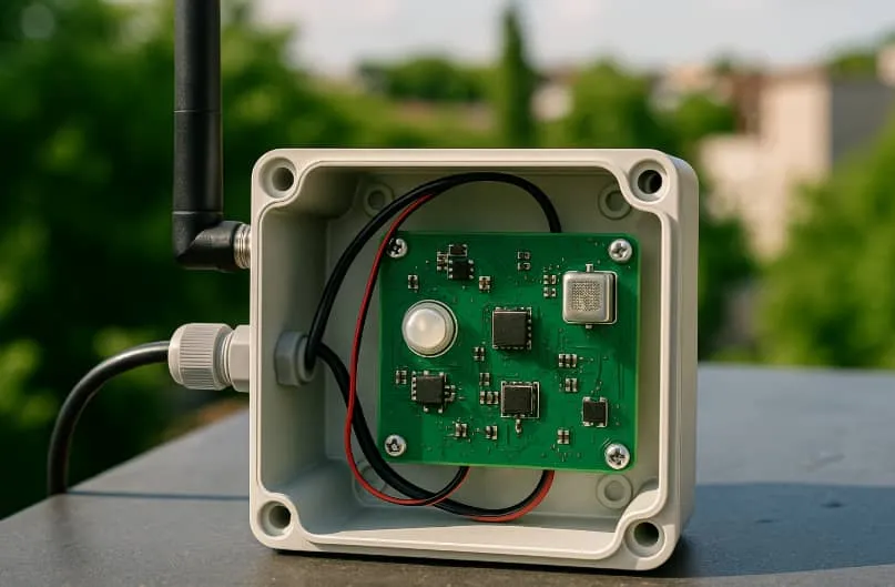
Industrial sensor PCBs operate in demanding conditions found in sectors like oil and gas extraction, mining operations, heavy manufacturing, and transportation systems. These environments expose electronics to extreme temperatures, intense vibrations, high humidity, corrosive chemicals, and mechanical shocks. Designing high-reliability industrial sensor PCBs requires a focus on robust PCB design to ensure uninterrupted data collection and signal processing. Failure in such systems can lead to costly downtime, safety risks, or inaccurate readings that compromise operational efficiency. Engineers must prioritize material choices, layout strategies, and protective measures tailored for harsh environment PCBs. This article explores key principles and best practices for creating vibration resistant PCBs and temperature resistant PCBs that meet rigorous performance demands.
Why High-Reliability Matters for Industrial Sensor PCBs
Sensors in industrial applications detect parameters such as pressure, temperature, flow, and vibration, feeding critical data into control systems. Harsh environments accelerate degradation mechanisms like delamination, solder joint fatigue, and trace cracking, reducing mean time between failures. Robust industrial PCB design extends operational life, minimizes maintenance, and supports predictive analytics for equipment health. Compliance with performance classes defined in standards like IPC-6012 ensures boards withstand cyclic stresses without compromising functionality. For electric engineers, understanding these factors informs trade-offs between cost, size, and durability during the design phase. Ultimately, high-reliability designs enable sensors to deliver precise measurements even under prolonged exposure to adverse conditions.
Key Challenges in High-Reliability PCB Design in Harsh Environment
Extreme temperatures cause thermal expansion mismatches between copper traces, laminates, and components, leading to microcracks and via failures. Vibrations induce fatigue in solder joints and mechanical stress on board edges, particularly in high-frequency oscillations common in machinery. Moisture and contaminants promote dendritic growth and electrochemical migration, shorting circuits over time. Dust and particulates exacerbate wear on connectors and increase thermal resistance. Engineers must address these through integrated solutions rather than isolated fixes. Balancing signal integrity for analog sensors with mechanical robustness defines successful industrial sensor PCB design.
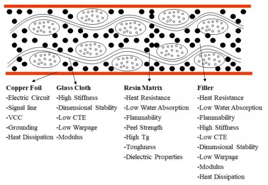
Material Selection for Temperature Resistant PCBs
Selecting laminates with high glass transition temperature prevents softening and warpage during thermal excursions. Materials engineered for low coefficient of thermal expansion minimize stress at interfaces with ceramic sensors or metal housings. Thicker copper weights improve current carrying capacity and heat dissipation in power sections. Multilayer constructions with controlled impedance stacks support high-speed sensor interfaces. Fabricators apply qualification tests to verify material stability under combined humidity and temperature cycles. This foundation supports overall robust PCB design in fluctuating thermal profiles. For detailed guidance on choosing substrates that meet IPC-4101 standards in demanding conditions, see our Understanding PCB Materials: A Guide to IPC-4101 Standards.
Here is a comparison of common materials for industrial sensor PCBs (approximate values):
| Material | Tg (°C) | CTE (z-axis, ppm/°C) | Key Advantages | Best Applications |
|---|---|---|---|---|
| Standard FR-4 | 130–140 | 50–70 | Low cost, good processability | Moderate environments |
| High-Tg FR-4 | 170–190 | 25–40 | Better thermal stability, lead-free compatible | General industrial sensors |
| Polyimide (PI) | 250–260 | 15–25 | Excellent flexibility & high-temp resistance | Extreme temperature & vibration |
| BT/Epoxy Blend | 180–200 | 30–40 | Low loss, good multilayer stability | High-speed sensor interfaces |
| Ceramic (Alumina/AlN) | >300 | Very low (~6–8) | Superior thermal conductivity & stability | High-power or ultra-harsh conditions |
High-Tg and polyimide options significantly outperform standard FR-4 in thermal cycling and vibration resistance. Thicker copper weights (2–4 oz) enhance current handling and heat dissipation in power sections. Qualification per IPC-4101 verifies stability under combined humidity and temperature stress.
Thermal Management Strategies in Industrial Sensor PCBs
Effective thermal design begins with strategic via placement under heat-generating components like amplifiers and ADCs. Filled or staggered vias reduce thermal resistance while maintaining structural integrity. Copper pours and polygons act as heat spreaders, channeling heat away from sensitive analog sections. Board thickness influences rigidity and convection, with 1.6 mm often serving as a baseline for industrial boards. Engineers simulate junction temperatures using finite element analysis to predict hotspots. Integrating these techniques ensures temperature resistant PCBs perform reliably across wide operating ranges.
Achieving Vibration Resistance in Harsh Environment PCBs
Wide traces and reinforced vias distribute mechanical loads, preventing rip-out during shock events. Component anchoring with epoxy or mechanical clips secures tall profiles against resonance. When selecting rugged components for these environments, consult our guide on Choosing the Right Parts for Industrial Automation PCBs. Stiffeners along board edges counteract flexing, especially near mounting holes. Solder joint geometry, such as fillet control, enhances fatigue life under cyclic loading. Layout avoids long unsupported spans that amplify vibrations. Vibration resistant PCB designs incorporate these elements to maintain electrical continuity in dynamic applications.
Conformal Coating for Protection in Harsh Environments
Conformal coating PCBs forms a thin barrier against moisture ingress, ionic contamination, and abrasion. Selective application over exposed areas preserves test points and connectors for field diagnostics. Curing methods ensure uniform thickness without bubbles that trap contaminants. Coatings compatible with rework processes allow component replacement without damage. Engineers evaluate coating properties for flexibility to accommodate thermal expansion. This step significantly boosts reliability for industrial sensor PCB design in humid or chemically aggressive settings.
EMI Shielding, Grounding, and Signal Integrity for Sensors
Industrial environments generate strong electromagnetic interference (EMI) from motors, drives, and machinery. Robust grounding uses solid planes with minimal splits to provide low-impedance return paths. Critical analog sensor traces should route as differential pairs with adjacent ground shielding or guard traces.
Power and ground plane segmentation isolates noisy digital sections from precision analog circuits. Stitching vias along trace edges maintain reference plane continuity. Decoupling capacitors placed close to IC pins suppress transients. These techniques preserve signal fidelity for low-level sensor outputs amid harsh EMI, ensuring accurate readings in vibration- and noise-prone settings.
High-Reliability PCB Layout Best Practices for Robust Design
Centralize high-vibration components near mounting points to shorten stress paths. Route critical sensor traces as differential pairs with ground shielding to preserve signal fidelity amid EMI from motors. Avoid right-angle bends that concentrate strain, opting for curved or 45-degree turns. Power and ground plane splits isolate noisy digital sections from precision analog sensors. Decoupling capacitors placed close to IC pins suppress transients exacerbated by environmental noise. These layout choices form the core of robust PCB design for sustained performance.
Suggested Reading: Optimizing Industrial Sensor PCB Layout for Signal Integrity and Noise Reduction
Testing and Qualification for High-Reliability Assurance
Environmental testing verifies designs through accelerated life cycles, including thermal shock and random vibration profiles. JEDEC standards guide temperature cycling protocols to assess intermetallic formation in joints. Board-level inspections confirm plating integrity and void-free soldermask. Functional testing under combined stresses simulates real-world deployment. Iterative qualification refines prototypes before production scaling. Adhering to IPC-A-600 criteria ensures visual and dimensional acceptability post-fabrication.
Real-World Case Studies and Lessons Learned
In oil & gas drilling sensors, switching to polyimide-based boards with filled thermal vias and conformal coating reduced field failures by extending MTBF in high-temperature, high-vibration environments. A mining vibration monitor project avoided solder joint fatigue by adding edge stiffeners and epoxy anchoring, cutting downtime costs significantly.
Lessons include the value of early FEA simulation for vibration hotspots and the importance of hybrid protection (coating + selective potting). Over-specifying materials without testing can inflate costs, while under-protecting leads to expensive recalls or safety incidents.
Conclusion
Designing high-reliability industrial sensor PCBs demands a holistic approach integrating material science, mechanical engineering, and electronics principles. Key strategies like advanced thermal management, vibration mitigation, and conformal coating directly address harsh environment challenges. Engineers benefit from structured adherence to proven standards for qualification. Implementing these practices yields durable, accurate systems that outperform in demanding applications. Forward-thinking designs not only meet current needs but anticipate evolving industrial requirements.
FAQs
Q1: What are the primary considerations for industrial sensor PCB design in high-vibration settings?
A1: Vibration resistant PCB designs prioritize wide traces, reinforced vias, and edge stiffeners to prevent fatigue. Component anchoring and balanced layouts reduce resonance amplification. Testing per established vibration profiles confirms joint integrity. These measures ensure signal stability for sensors monitoring dynamic processes.
Q2: How does conformal coating enhance harsh environment PCB reliability?
A2: Conformal coating PCBs protects against moisture, chemicals, and dust by forming a dielectric barrier. It prevents corrosion and arcing in humid conditions common to industrial sites. Proper application thickness and curing maintain flexibility for thermal cycling. This boosts mean time to failure for exposed assemblies.
Q3: Why is material selection critical for temperature resistant PCBs?
A3: High glass transition temperature laminates resist warpage and delamination in thermal extremes. Low CTE materials match component expansion to minimize stress. Thicker foils aid heat dissipation from sensor circuits. Qualification under combined environments verifies long-term stability.
Q4: What role do standards play in robust PCB design validation?
A4: Standards like IPC-6012 define performance classes for high-reliability boards, specifying tolerances for harsh exposures. They guide thermal and mechanical testing protocols. Compliance ensures consistency across supply chains. Engineers use them to benchmark designs against proven benchmarks.
References
IPC-6012E — Qualification and Performance Specification for Rigid Printed Boards. IPC, 2017
IPC-A-600K — Acceptability of Printed Boards. IPC, 2020
JEDEC JESD22-A104 — Temperature Cycling. JEDEC, 2009


