










PCB Teardrops: Critical Reinforcement for Trace Reliability in Manufacturing
What This Video Covers
PCB teardrops — the tapered copper reinforcements added at the junction between traces and pads or vias. Often overlooked, these small features significantly enhance manufacturing reliability by protecting against drill offset, etching variations, and mechanical stress.
Teardrops widen the connection point, making it more tolerant to misalignment during PCB fabrication, especially in the dense HDI PCB design, fine traces, and small vias. Without them, even minor shifts can sever traces or create weak points that lead to cracks and field failures.
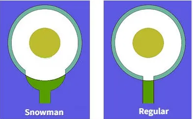
The video reviews different teardrop styles (standard and "snowman" shapes), practical design rules — such as keeping length 1–2 times the trace width while avoiding sharp expansions — and when to limit or skip them on high-speed signals. Proper use of teardrops improves overall board reliability during PCB prototype and PCB mass production.
These design details matter across demanding applications including medical devices PCB, automotive PCB, and aerospace PCB. Understanding teardrops helps engineers reduce defects and achieve better yields when ordering PCB assembly.
Key Highlights
- Teardrops reinforce trace-to-pad and trace-to-via junctions, protecting against drill misalignment and etching issues common in PCB fabrication.
- Use teardrops on most connections in fine-pitch and dense layouts, keeping length 1–2× trace width while verifying spacing with DRC.
- In high-speed or ultra-dense designs, carefully control or skip teardrops to maintain signal integrity without compromising manufacturability.
Common Manufacturing Challenges Without Proper Teardrops
In high-volume PCB fabrication, even slight drill wander or registration errors can disconnect narrow traces from pads, particularly on boards with 0.1 mm or smaller features. Etching tolerances further exacerbate this by undercutting copper at junctions, resulting in necking or complete opens that only appear after assembly or during thermal cycling.
Without teardrops, manufacturers frequently observe higher scrap rates in fine-pitch BGA and QFN packages where pad-to-trace interfaces are most vulnerable. These defects contribute to costly rework, delayed time-to-market, and potential reliability issues in the field, such as intermittent connections under vibration or temperature extremes.
Practical production data shows that boards designed without adequate teardrop reinforcement often require tighter process controls and more frequent tooling adjustments, increasing overall fabrication costs.
Optimal Teardrop Design Rules and Guidelines
Effective teardrop implementation follows established DFM principles. The teardrop length should typically range from 1 to 2 times the trace width, with a smooth taper angle that avoids abrupt geometry changes capable of creating stress concentrations. Designers must maintain minimum spacing rules to prevent solder mask or copper shorts in dense areas.
Advanced EDA tools automatically generate teardrops, but manual verification remains essential for high-reliability designs. Overly large teardrops can violate clearance constraints in HDI builds with microvias, while undersized ones provide insufficient protection.
Production teams recommend running full DRC checks with teardrops enabled and reviewing Gerber files to confirm actual copper geometry matches design intent before releasing for fabrication.
Teardrop Impact on High-Density and High-Speed PCB Designs
In HDI and multilayer constructions, teardrops become especially valuable for maintaining connectivity through multiple lamination cycles and precise laser drilling. However, they introduce minor parasitic effects that must be modeled in high-speed applications.
Signal integrity simulations often reveal slight impedance discontinuities at teardrop locations on critical traces above 5 GHz. Engineers address this through selective application — using teardrops on power and ground connections while optimizing or omitting them on differential pairs after careful analysis.
Balanced implementation ensures manufacturability without sacrificing electrical performance, delivering boards that pass both functional testing and environmental qualification.
Teardrop Selection and Application Across Industries
| Application | Recommended Teardrop Usage | Key Considerations | Typical Benefits |
|---|---|---|---|
| Automotive PCB | Full coverage on most junctions | Vibration and thermal cycling resistance | Reduced field failures |
| Medical Devices PCB | Conservative sizing on fine traces | High reliability and biocompatibility | Improved yield consistency |
| Aerospace PCB | Mandatory on all critical nets | Extreme environment tolerance | Enhanced long-term durability |
| Consumer Electronics | Selective on dense areas | Cost-sensitive production | Balanced DFM and performance |
Real-World Failure Modes and DFM Mitigation Strategies
Common failures linked to missing or inadequate teardrops include trace lifting during wave soldering, annular ring breakout after drilling, and micro-cracks that propagate under repeated thermal stress. These issues frequently surface during ICT or flying probe testing and can lead to batch rejection.
DFM best practices involve early collaboration between design and fabrication teams to define teardrop parameters in stack-up documentation. Fabricators can also apply process-specific adjustments, such as optimized etch compensation, when teardrops are properly specified.
Proactive verification through design reviews and prototype builds significantly lowers defect rates and supports smoother transition to mass production. Consistent application of these strategies results in higher first-pass yields and more robust end products.
FAQ
Q1: When should you add teardrops to PCB traces and pads?
A1: Add teardrops at nearly all trace-to-pad and trace-to-via connections, especially in fine-pitch, HDI, or multilayer boards where drill offset risk is higher.
Q2: What problems occur without teardrops on PCBs?
A2: Without teardrops, minor drill misalignment or manufacturing tolerances can sever traces or create weak points prone to cracking under thermal or mechanical stress.
Q3: Do teardrops affect high-speed or dense PCB designs?
A3: Yes — while beneficial for reliability, they should be controlled or omitted on critical high-speed traces to avoid impedance changes or spacing violations.
Q4: How do teardrops influence PCB fabrication yields?
A4: Properly implemented teardrops improve fabrication yields by increasing tolerance to registration errors and etching variations, particularly beneficial for complex boards with small features. This reduces scrap and supports more predictable production schedules.
Q5: What is the recommended teardrop size relative to trace width?
A5: Industry practice suggests teardrop lengths of 1–2 times the trace width with a gradual taper. Exact dimensions should be verified against the chosen fabricator’s capabilities and the board’s overall density to maintain design rule compliance.
See those tiny "tears" on a PCB? They're not decoration—they're teardrops.
They're added because trace-to-pad corners are weak.
A teardrop is a tapered copper transition between a trace and a pad or via.
It widens that spot, making it more tolerant to drill offset and stress.
Without it, a small shift can cut a trace or cause cracks.
This gets worse with fine traces, small vias, and dense layouts.
You'll also see different styles, like standard shapes or "snowman" types.
So here are some practical design guidelines:
Use teardrops at trace-to-pad and via connections.
Keep length around one to two times trace width, and avoid sharp expansion.
Skip or control them carefully on high-speed or very dense traces.
Most PCB tools can auto-generate them, but always verify spacing with DRC before release.





