00:53
PCB Impedance
PCB impedance refers to the opposition to alternating current flow in printed circuit boards, a critical factor in ensuring signal integrity and performance in high-speed electronic designs. For engineers and designers searching for information on PCB impedance, this tag serves as a comprehensive resource that delves into the principles, calculations, and real-world implications of impedance control. Understanding impedance is essential for preventing issues like signal reflections, crosstalk, and electromagnetic interference, which can degrade the functionality of circuits in applications such as telecommunications, computing, and automotive electronics. By maintaining controlled impedance, designers can achieve reliable data transmission at gigabit speeds, making it indispensable for modern PCB layouts involving differential pairs, transmission lines, and multilayer boards. In practice, achieving optimal PCB impedance involves selecting appropriate trace geometries, dielectric materials, and stackup configurations. For instance, tools like impedance calculators help determine trace width and spacing based on target values, typically 50 ohms for single-ended signals or 100 ohms for differential pairs. Best practices include simulating designs with software such as Altium or KiCad to verify impedance before fabrication, and collaborating with manufacturers to specify tolerances that align with industry standards like IPC-2141. This approach not only minimizes prototyping iterations but also enhances overall board reliability, reducing costs and time to market for projects ranging from consumer gadgets to industrial systems. The articles gathered under the PCB Impedance tag provide in-depth guidance on these topics, from beginner-friendly explanations of characteristic impedance to advanced techniques for mitigating impedance mismatches in RF and high-frequency circuits. Whether you are troubleshooting a design flaw or optimizing a new prototype, these resources offer practical strategies to apply impedance concepts effectively in your work.
Video Guide

Technical Articles
How PCB CAM Resolves Conflicting Impedance Control Requirements
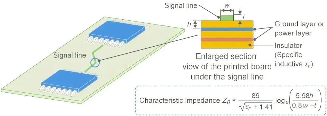
Revealing the "Pseudo Eight-Layer" Stackup: Can a Six-Layer PCB Deliver Eight-Layer Performance?
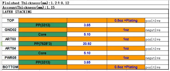
PCB Impedance Calculation for Signal Integrity
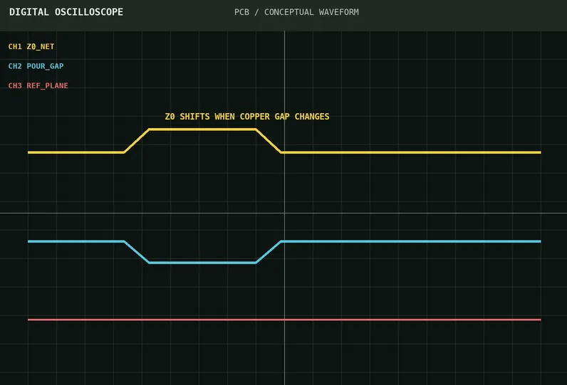
Why Impedance Changes After Adjacent Copper Pour Even When Trace Width Does Not
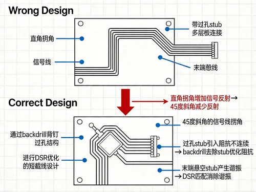
Signal-Integrity Simulation: Five Places Designs Usually Break

Definition and Design Purpose of Characteristic Impedance in PCBs

Impedance Calculation Parameters: FR4 Substrate, Copper Thickness, and Prepreg

PCB Impedance Control: Manufacturing Factors and Parameter Relationships

Impedance Design Software and Calculation Mode Selection
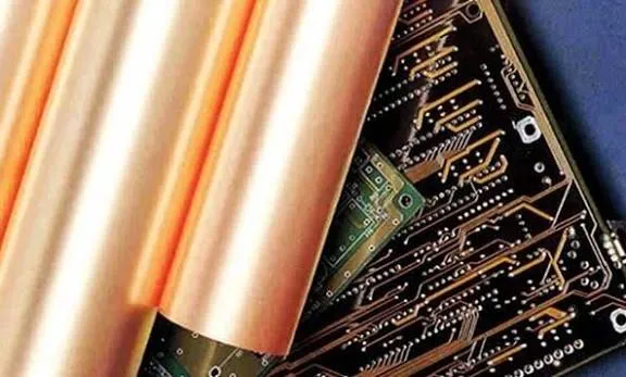
Why Are PCB Copper Foil Thicknesses Different?
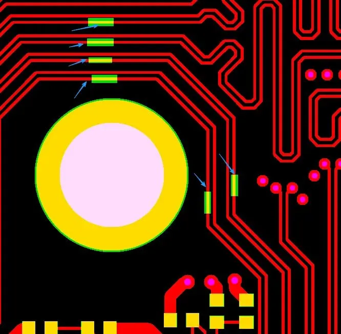
Why Do PCB Impedance-Controlled Traces Sometimes Require Local Solder Mask Openings?
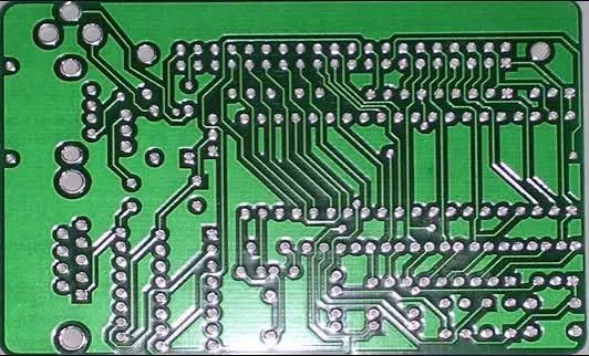
Why Does a PCB Designed for 50 Ω Measure 53 Ω After Manufacturing?
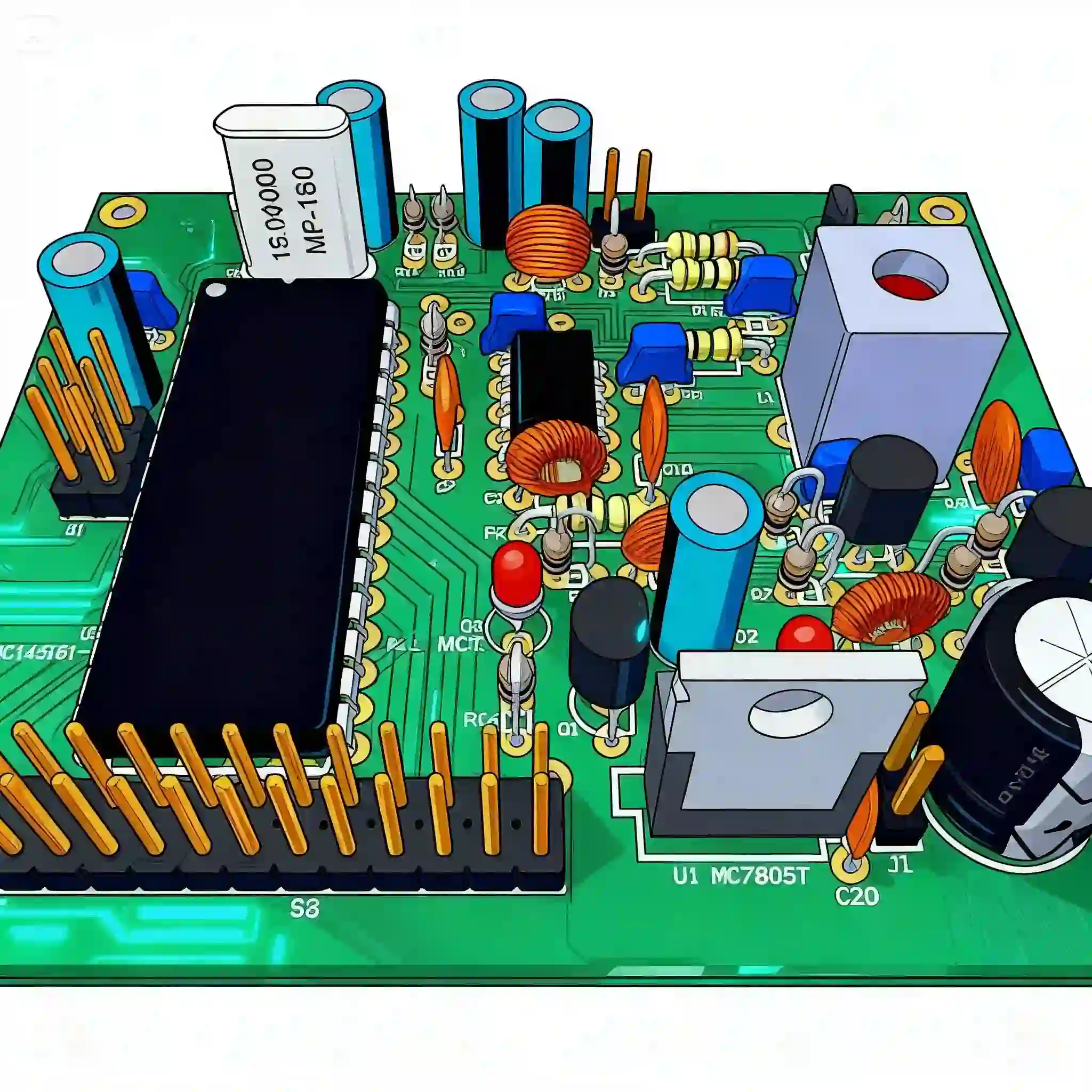
Enhancing USB PCB Performance: A Guide to Optimal PCB Layout and Signal Integrity
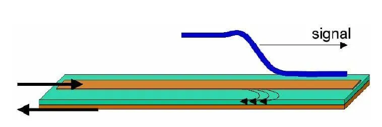
DIY PCB Impedance Measurement: A Home Lab Guide
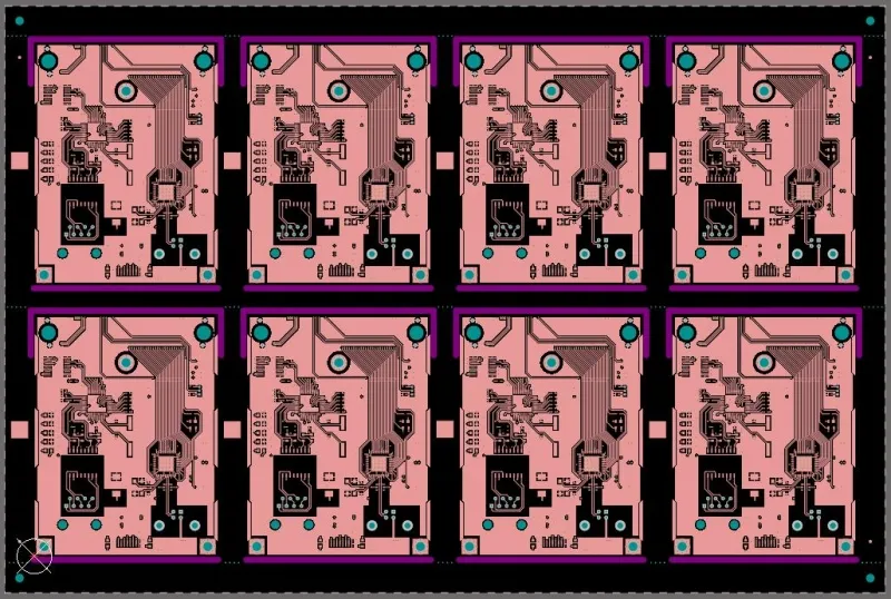
PCB Panel Size and Impedance Control: Design Considerations
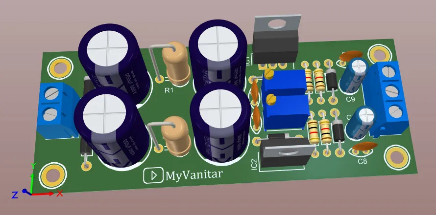
Best Practices for Power Supply PCB Trace Routing
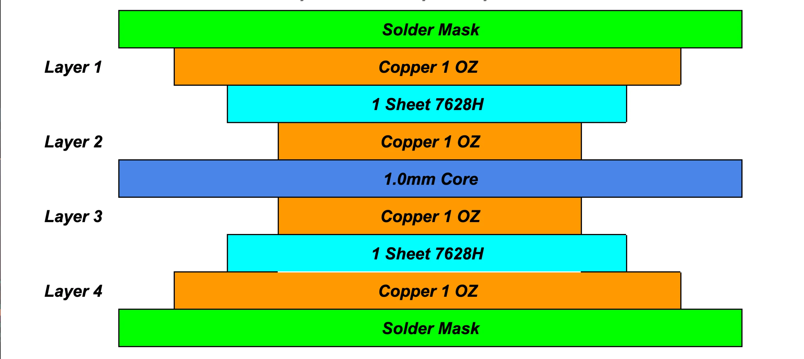
4 Layer PCB Stackp: A Practical Tutorial for Simple Designs
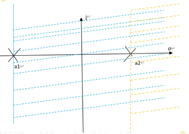
Pole-Zero Analysis in Analog Circuits (Part 2)
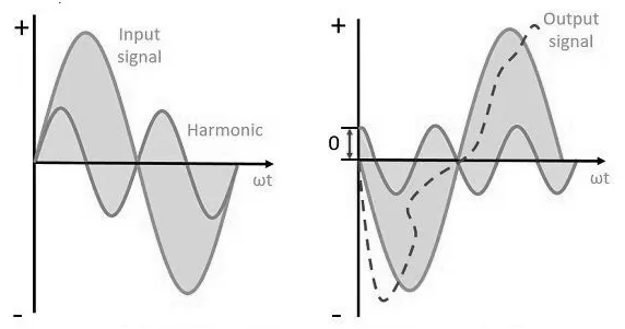
Types of Amplifier Distortion and How to Reduce Them