Introduction
Copper layer thickness stands as a critical parameter in high current PCB design, directly impacting the board's ability to handle power without failure. Engineers optimizing PCB trace thickness current must consider how thicker copper reduces resistance and supports higher amperage loads while improving PCB heat dissipation. In applications like power supplies and motor drives, inadequate thickness leads to excessive heating, degrading components and shortening lifespan. Effective PCB thermal management relies on strategic copper layer thickness selection to spread heat efficiently across the board. This article delves into the engineering principles, standards, and best practices for balancing these factors. By understanding these relationships, designers can achieve robust performance aligned with industry requirements.
Why Copper Layer Thickness Matters in PCB Design
Copper layer thickness determines the cross-sectional area of traces, fundamentally affecting current carrying capacity and thermal performance. Thinner foils, common in high-density signal layers, limit current due to higher resistance and poorer heat spreading, risking hotspots in power sections. Conversely, thicker copper enables high current PCB design by lowering resistivity and enhancing conduction away from sources. Industry data shows that neglecting this parameter contributes to a significant portion of field failures in power electronics. PCB thermal management becomes challenging without sufficient thickness, as heat accumulates locally rather than dissipating broadly. Optimizing thickness ensures compliance with reliability standards and extends operational margins.
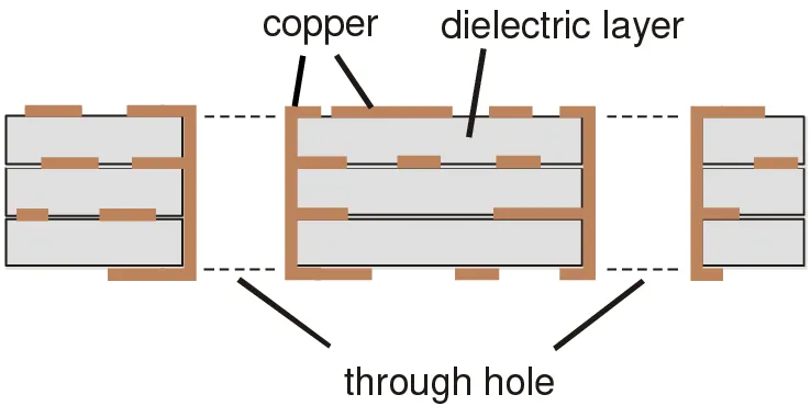
In multilayer boards, outer layers often benefit from thicker copper for better external convection, while internal layers prioritize plane distribution. This differentiation underscores the need for layer-specific planning during stackup development. Engineers must evaluate maximum expected currents early to avoid costly respins. The interplay between PCB trace thickness current limits and overall board temperature rise demands integrated analysis.
Technical Principles of Current Capacity
Current capacity in PCB traces follows from basic electrical principles, where resistance R equals resistivity rho times length L divided by cross-sectional area A. Since A is width times thickness, increasing copper layer thickness directly reduces R, allowing higher currents before excessive I squared R heating occurs. Standard copper weights start at 1 oz per square foot, approximately 35 microns thick, providing baseline capacity for most designs. For demanding loads, 2 oz or 3 oz foils double or triple this thickness, proportionally boosting capacity. The IPC-2152 standard provides detailed charts accounting for variables like external versus internal traces, ambient temperature, and allowable rise, superseding older methods.
These charts reveal that for a given temperature rise, say 20 degrees Celsius, thicker copper permits narrower traces or higher currents, optimizing space. External traces dissipate heat better due to air exposure, unlike embedded ones surrounded by dielectric. Board thickness and copper coverage also influence results, as denser planes aid spreading. Designers use IPC-2152-derived calculators to interpolate values precisely during layout.
Mechanisms of Heat Dissipation in PCBs
PCB heat dissipation relies on conduction through copper, convection to air, and radiation, with copper layer thickness enhancing the primary path. Copper's high thermal conductivity, around 400 W/mK, far exceeds FR-4's 0.3 W/mK, making thicker layers effective heat spreaders. Heat from components flows laterally along traces and planes, with spreading effectiveness increasing with thickness due to larger volume. Thinner layers confine heat, raising local temperatures and risking delamination or electromigration. In high current scenarios, this mechanism prevents hotspots by distributing thermal load.
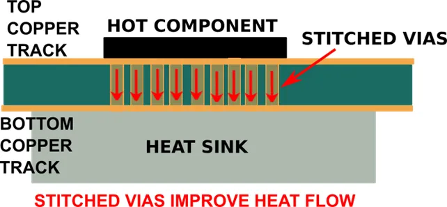
Multilayer designs leverage plane layers for uniform dissipation, but vias bridge layers to transfer heat vertically. The IPC-2221 standard outlines design practices for thermal management, including conductor sizing and spacing to promote airflow. Finite element analysis confirms that doubling thickness can reduce peak temperatures substantially by improving conduction paths. Environmental factors like airflow further amplify benefits of optimized thickness.
Best Practices for Optimizing Copper Layer Thickness
Begin high current PCB design by estimating peak currents and desired temperature rises using IPC-2152 guidelines to select minimum thickness. Specify 2 oz or heavier on power layers while keeping signal layers at 1 oz to balance cost and manufacturability. Widen traces where possible, as capacity scales with both dimensions, but prioritize thickness for compact layouts. Incorporate solid copper pours around high-power components to maximize spreading area.
For PCB thermal management, array thermal vias under hotspots, plating them with thick copper to enhance conduction between layers. Use multilayer stackups with dedicated power and ground planes adjacent to signal layers for symmetric heat paths. Simulate thermal profiles early, adjusting thickness iteratively to meet margins. Avoid over-thickening beyond needs, as foils over 3 oz complicate etching and increase material costs. Validate designs against IPC-6012 performance specifications for copper integrity post-fabrication.
Tradeoffs include higher impedance in thin high-speed traces, so segregate power and signal sections. Factory capabilities limit maximum thickness, typically to 4-6 oz, requiring early supplier consultation. Iterative prototyping with infrared imaging confirms predictions.
Insights from High Current PCB Applications
In power converter designs, switching to thicker outer copper layers reduced trace temperatures by leveraging natural convection. Internal planes handled distribution, minimizing voltage drops. Engineers observed that combining 2 oz traces with vias lowered overall board rise, aligning with IPC-2152 predictions. Troubleshooting overheating often traces back to underestimated currents or thin foils, resolved by up-speccing thickness. These examples highlight systematic optimization over ad-hoc fixes.
Conclusion
Optimizing copper layer thickness elevates PCB trace thickness current limits and strengthens PCB thermal management, ensuring reliability in demanding environments. Key principles from resistance reduction to heat spreading guide selections per IPC standards. Practical steps like via integration and simulation yield efficient high current PCB designs. Prioritizing these factors minimizes risks and enhances performance. Designers achieve superior outcomes by integrating thickness decisions early in the process.
FAQs
Q1: How does PCB trace thickness current capacity change with copper layer thickness?
A1: Increasing copper layer thickness enlarges the trace cross-section, reducing resistance and allowing higher currents for the same temperature rise, as detailed in the IPC-2152 standard. For instance, doubling from 1 oz to 2 oz can support substantially more amperage in external traces. This principle aids high current PCB design while maintaining compact layouts. Always factor in board conditions for accurate sizing.
Q2: What role does copper layer thickness play in PCB thermal management?
A2: Thicker copper improves PCB heat dissipation through superior conduction and spreading, lowering peak temperatures around components. It enables efficient transfer to outer surfaces for convection. In multilayer boards, this pairs with planes for uniform distribution. Adhering to IPC-2221 practices ensures effective thermal paths without excessive material use.
Q3: Why choose thicker copper for high current PCB design?
A3: High current PCB design demands thicker copper to handle amperage without I squared R losses causing failures. It boosts capacity per IPC-2152 charts and aids thermal management. While costlier, benefits outweigh in power applications. Balance with width and vias for optimal results.
Q4: How can engineers optimize PCB heat dissipation with layer thickness?
A4: Select copper layer thickness based on simulated max loads, using 2 oz or more for power paths. Add thermal vias and pours to enhance spreading. IPC-6012 verifies post-fabrication integrity. This approach minimizes hotspots and supports reliable operation.
References
IPC-2152 — Standard for Determining Current-Carrying Capacity in Printed Board Design. IPC, 2009
IPC-2221B — Generic Standard on Printed Board Design. IPC, 2012
IPC-6012E — Qualification and Performance Specification for Rigid Printed Boards. IPC, 2017


