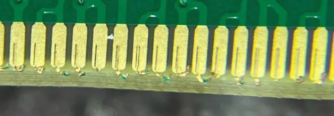
When a PCB arrives, you may inspect it under a bright light and notice a reddish tint around the vias or copper-colored patterns showing through large copper areas. Your first reaction may be: "Is the copper exposed?"
Not necessarily. This appearance may be what the PCB industry commonly calls false copper exposure.
The two conditions differ by only one word, but their implications are completely different. True copper exposure is a physical defect that can affect reliability and safety. False copper exposure is primarily a visual concern caused by the appearance of copper beneath an intact solder mask.
The Fundamental Difference: Is the Copper Physically Exposed?
True copper exposure occurs when the solder mask contains a hole, crack, scratch, or missing area that directly exposes the copper layer to the surrounding environment. Once the solder mask barrier is damaged, electrical isolation is compromised. The exposed area may increase the risk of short circuits, oxidation, contamination, and other reliability problems, making it a substantive quality defect.
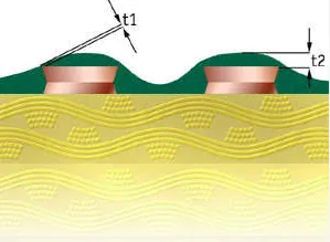
False copper exposure is different. The solder mask still continuously covers the copper surface and has no physical break. The copper color or texture is visible because the solder mask is locally too thin, has insufficient hiding power, or has relatively strong light transmission. The copper tone therefore appears to show through the coating even though the copper remains physically protected.

A simple analogy is a raincoat. True copper exposure is like a hole in the raincoat that allows water to reach the clothing underneath. False copper exposure is like a raincoat made from very thin material: the color of the clothing can be seen faintly, but water still cannot pass through.
The key distinction is whether the copper remains physically isolated and protected by the solder mask.
Four Practical Ways to Identify the Condition
1. Fingernail Test
Gently run a fingernail across the suspected area.
- A false copper exposure area should feel smooth and even, without a noticeable step, pit, or opening.
- A true exposed-copper area may feel uneven. You may be able to detect a break in the solder mask or the rougher surface of the exposed copper.
This is a quick preliminary check, but it should be performed gently so that an otherwise intact solder mask is not damaged during inspection.
2. Oblique Bright-Light Inspection with Magnification
Use a bright LED light and inspect the area from an angle. A 3× to 10× magnifying glass or a stereo microscope can make the distinction easier to see.
- With false copper exposure, the solder mask remains continuous and intact. The copper color appears to show through the coating.
- With true copper exposure, you may see microcracks, pinholes, or a clearly defined area where the copper is no longer covered by solder mask.
Oblique illumination is useful because it reveals changes in surface continuity and makes small cracks or coating defects easier to distinguish from simple color variation.
3. Adhesive-Tape Peel Test
For a more practical check, use a high-tack test tape such as 3M 610. Press the tape firmly onto the suspected area and peel it quickly at an angle of approximately 45°.
- If no copper or solder-mask material transfers to the tape, the solder-mask adhesion is likely intact, and the condition is probably false copper exposure.
- If fragments of solder mask or copper particles are removed by the tape, the area requires close attention because the coating or copper surface may not be properly bonded.
This test should be applied in accordance with the inspection procedure for the product. It is a screening method rather than a replacement for cross-sectional analysis when the result is uncertain or the product has stringent reliability requirements.
4. Microsection Analysis
For critical products, metallographic microsectioning is the most definitive method. A cross-section can be examined under a microscope to measure the actual solder-mask thickness and verify whether the coating remains continuous over the copper.
In one reported case, the solder mask near a via was only 5.77 μm thick, while the thickness in a more uniform area was 18.35 μm. Such a large local difference makes false copper exposure much more likely. A microsection report replaces visual judgment with measurable evidence and can help determine whether the issue is related to coating thickness, coverage, or a true break in the solder mask.
What to Do After Finding the Problem
If the Condition Is False Copper Exposure
Under IPC-A-600, slight visibility of the copper color is generally acceptable when the solder mask remains continuous and intact, without cracking, blistering, or delamination.
Acceptance should still be evaluated against the applicable drawing, purchase specification, and product reliability requirements. For automotive electronics, medical equipment, and other high-reliability applications, it is advisable to specify IPC Class 3 in the purchase documentation and define solder-mask thickness requirements where appropriate. Clear requirements can reduce the probability of excessive copper show-through at the manufacturing stage.
False copper exposure may not represent an immediate electrical failure, but an unusually thin or poorly covered solder mask can provide less process and environmental margin. Therefore, recurring or widespread appearance issues should be reviewed with the PCB manufacturer rather than dismissed solely because the copper is not physically exposed.
If the Copper Is Truly Exposed
The location and size of the defect must be evaluated.
According to the criteria described here, exposed copper is not permitted on traces, conductor sidewalls, or at hole openings. For other areas, the exposed-copper dimension should be no greater than 0.25 mm, should not exceed 20% of the spacing between adjacent conductors, and should occur no more than three times per side of each panelized board. Any defect exceeding the applicable limit should be reviewed with the PCB manufacturer for rework or scrap disposition.
Large exposed-copper areas are particularly unsuitable for acceptance without evaluation because they can compromise insulation and increase the possibility of oxidation, contamination, or unintended electrical contact.
Why Does False Copper Exposure Occur?
Understanding the causes helps prevent the problem during PCB fabrication and specification.

Insufficient Solder-Mask Thickness
Insufficient or nonuniform solder-mask thickness is the primary cause. If the coating is locally too thin, its hiding power decreases after curing and the copper color becomes visible through the surface. Variations in coating distribution can make the effect appear only in certain regions of the board.
Via Plugging and Solder-Mask Coverage Issues
Via-processing conditions are another common cause. If via plugging is not specified, solder-mask printing may be performed directly over vias without filling the holes with ink. After thermal processing, the area may show a copper-colored appearance because the ink has not provided sufficient coverage inside or around the via.
Insufficient alignment of the aluminum screen, or an inappropriate squeegee pressure or angle, can also prevent the ink from entering and covering the via area properly. These process conditions may produce locally thin coverage even when the surrounding solder mask appears normal.
Thick Copper
Boards with heavy copper, generally copper thickness of 2 oz or more, are more susceptible to this visual effect. The greater height difference between the copper surface and the laminate creates a more difficult coating profile. Under a constant screen-printing pressure, the solder mask over the conductors may become relatively thin. The area can then take on a yellow or reddish appearance, creating the impression of exposed copper.
Practical Inspection Sequence
When a copper-colored area is first noticed, avoid immediately classifying it as a defect. Begin with a gentle surface inspection, follow with bright-light examination under magnification, and then perform an adhesive-tape test if the product procedure permits. If the result remains uncertain—or if the board is intended for a high-reliability application—request a microsection analysis from the PCB manufacturer.
In short, true copper exposure means that the protective barrier has failed, whereas false copper exposure is a visual effect caused by the copper showing through an intact solder mask. The distinction can often be made quickly with a fingernail check, focused lighting, and tape testing, but a cross-sectional report is the most reliable way to resolve difficult cases.