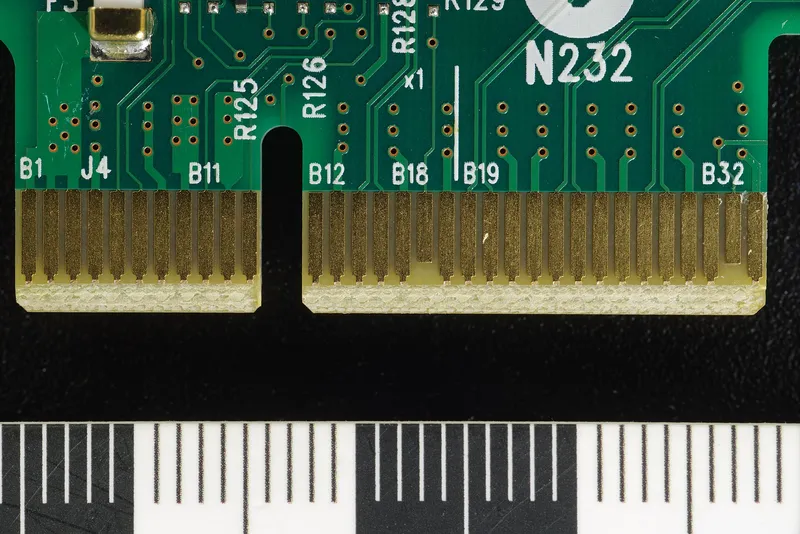
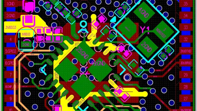
Printed circuit boards sit at the center of modern electronics. One small specification — copper thickness — affects how the board conducts current, spreads heat, and holds up mechanically over its life.
This article looks at the role of copper thickness in PCB fabrication.
What PCB Copper Thickness Means
In fabrication, copper thickness is the thickness of the copper foil. It is commonly specified in ounces (oz), meaning the weight of copper per square foot. Typical values are:
- 17.5 μm (0.5 oz)
- 35 μm (1 oz)
- 70 μm (2 oz)
Different thicknesses serve different electrical requirements and applications. Figures 1 through 3 cover three main effects on the board.
Copper Thickness Sets Current-Carrying Ability
Copper is the main conductor on a PCB. Changing its thickness changes how well the board can carry current.
If the copper is too thin, current capacity drops, and signal attenuation and unstable voltage become more likely.
If the copper is too thick, conduction improves, but cost and process difficulty rise. Heavy copper can also increase resin flow during lamination and create fabrication defects.
Design note: 1 oz copper is the usual choice for ordinary boards. Special needs such as high current can justify evaluating 2 oz, provided the process can support it.
Copper Thickness Affects Heat Spreading
As device power rises, heat spreading becomes more important.
Copper conducts current and also conducts heat. Thicker copper spreads heat faster and more evenly, which helps lower component surface temperature and can extend service life.
Besides choosing an appropriate thickness, unused areas can be poured with copper to add heat-spreading paths and raise the board's overall thermal efficiency.
Copper Thickness Affects Mechanical Stability
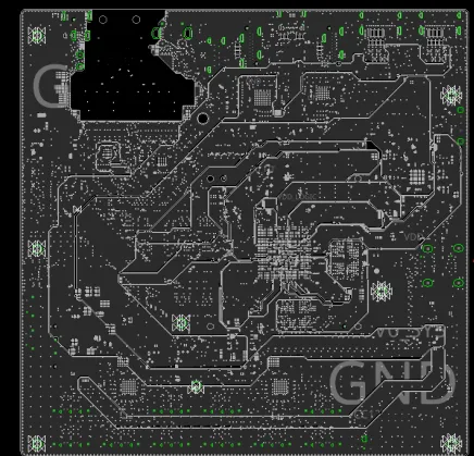

A PCB is a conductive network and also part of the mechanical structure.
- An appropriate copper thickness can raise bending resistance and reduce cracking and solder-joint lift over long use.
- It can also increase pad strength, improve solder reliability, and reduce cold or incomplete joints.
Copper thickness is especially important on products that need higher mechanical strength, such as automotive and industrial-control boards.
Summary
Copper thickness is a small specification with a large effect. A well-built PCB usually has a copper weight that fits the job:
- Stable conduction requires copper that is not too thin
- Fast heat spreading requires copper that is not under-specified
- Mechanical strength requires copper that is not ignored
Choose thickness from function, current, thermal need, and fabrication cost together, and pick the value that fits the design.