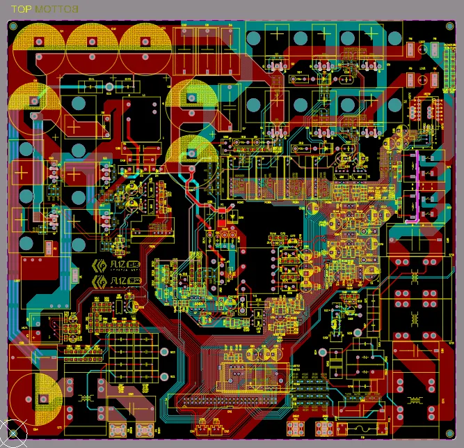
Server, industrial control, and consumer PCBs are all manufactured using the same fundamental PCB processes, but their design priorities differ substantially. The application environment, expected service life, electrical performance, material system, layer count, testing requirements, and cost targets all influence the final board structure.
The values described below represent typical characteristics rather than universal specifications. Actual requirements depend on the product architecture, interface speed, operating environment, reliability target, and customer acceptance criteria.
Core Differences Among the Three PCB Categories
1. Application Environment and Service Life
Server PCBs are commonly deployed in data centers and may operate continuously, 24 hours a day and 7 days a week. They must support high data throughput while maintaining stable electrical performance and thermal behavior. Signal integrity and power integrity are major design concerns because high-speed interfaces, dense routing, and large transient currents can all affect system reliability. A typical design life is approximately 7–10 years.
Continuous operation also means that heat cannot be treated as a secondary issue. The PCB must work with the system cooling architecture to control temperature rise in high-power areas. Excessive temperature can increase material stress, accelerate aging, and affect the electrical characteristics of high-speed interconnects. Consequently, server boards usually require more rigorous stackup planning, impedance control, power-distribution design, and manufacturing inspection.
Industrial control PCBs are designed for equipment that may operate in harsh environments. Depending on the application, the board may be exposed to high humidity, dust, vibration, temperature cycling, and electrical interference. Industrial systems are often expected to remain in service for more than 10 years, so long-term mechanical and electrical stability is usually more important than minimizing initial cost.
Environmental reliability affects both material selection and construction. Moisture and contamination can increase the risk of leakage or electrochemical migration, while vibration places additional stress on solder joints, connectors, and plated-through holes. The board therefore needs sufficient structural strength and materials that can withstand the intended operating conditions.

Consumer electronics PCBs are generally used in relatively controlled environments and are often designed for shorter product lifecycles, commonly around 2–5 years. The operating conditions are usually less demanding than those of servers or industrial equipment, although exceptions exist. Consumer products prioritize compact size, rapid production, appearance, and low unit cost. These priorities often lead to simpler layer structures and more cost-sensitive material and surface-finish choices.

2. Materials and Manufacturing Processes
Server boards commonly use low-loss, high-speed laminate systems, such as Panasonic M6 or M7 materials, when the design requires controlled high-frequency performance. As data rates increase, dielectric loss and conductor loss can significantly affect insertion loss and waveform quality. The material system must therefore be selected together with the stackup, trace geometry, copper roughness, and impedance target.
High-density interconnect, or HDI, construction is also common in server applications. Backdrilling can remove unused portions of plated through-holes that would otherwise behave as stubs and create signal discontinuities. Via-in-pad structures and resin-filled vias can support dense component escape routing and reduce the impact of complex interconnect geometry. These processes do not automatically guarantee good signal integrity, but they provide additional control over the electrical path when correctly integrated into the design.
Industrial control boards place greater emphasis on high glass-transition-temperature materials and resistance to conductive anodic filament, or CAF, growth. High-Tg laminates, including materials with a Tg above 170 °C, can provide better resistance to thermal stress during fabrication and operation. CAF resistance is important in environments where moisture, electric fields, and closely spaced conductors could otherwise contribute to internal conductive paths.
Industrial boards may also use relatively heavy copper, with 2 oz copper often used as a starting point for designs requiring higher current capacity. A board thickness of 2.0 mm or more is common in some industrial constructions because increased thickness can improve mechanical rigidity and support demanding connector or mounting conditions. These values are application-dependent and should not be treated as mandatory rules for every industrial PCB.
Consumer products generally use conventional FR-4 materials when the electrical and environmental requirements do not justify more specialized laminates. Design rules are often less aggressive, with line widths and spaces greater than 0.1 mm in many cost-sensitive designs. Thin boards, compact form factors, and economical surface finishes such as hot air solder leveling, or HASL, are commonly selected to reduce manufacturing cost.
However, a consumer PCB may still require advanced materials or fine geometries if it contains high-speed interfaces, compact wireless circuitry, or demanding thermal structures. Product category alone does not determine the material system; the actual electrical and mechanical requirements remain decisive.
3. Layer Count and Structural Features
Server PCBs commonly have high layer counts, typically around 16–40 layers in the type of construction described here. Multiple power and ground planes help distribute current and provide controlled reference structures for high-speed signals. Dense routing often requires microvias, sequentially built HDI structures, via-in-pad technology, and multiple levels of blind and buried vias.
Typical server board thicknesses are approximately 2.0–3.2 mm. The stackup must balance routing density, controlled impedance, power delivery, thermal behavior, manufacturability, and mechanical strength. A signal trace cannot be considered independently from its reference plane and dielectric structure, so layer assignment and plane continuity are essential parts of the design.
Industrial control boards commonly use approximately 8–16 layers. Their design rules are often more conservative, and relatively large finished hole diameters, such as those above 0.3 mm, may be acceptable. The additional spacing and larger features can improve manufacturing robustness and support long-term reliability under mechanical and environmental stress.
Consumer PCBs are frequently built with 2–8 layers and thicknesses of approximately 0.6–1.6 mm. Their routing may use wider line-and-space rules, while the overall board is optimized for compactness and cost. Although the construction is often simpler, the layout may be physically dense because components must fit into a small enclosure. This creates a different type of design challenge: the board may have fewer layers, but placement, routing, thermal spreading, and assembly constraints can be tightly coupled.
4. Testing Requirements and Cost
Server PCBs generally undergo extensive inspection because a field failure can interrupt critical computing or storage services. The described test flow includes 100% four-wire flying-probe testing for detecting very small shorts, X-ray inspection of backdrill depth, and aging testing. These tests address different risks: electrical continuity and isolation, the geometry of high-speed interconnect features, and stability after extended operation.
Because server boards combine high layer counts, specialized laminates, HDI structures, backdrilling, tight impedance requirements, and extensive testing, their unit cost can reach several thousand yuan per square meter or more, depending on the construction and production conditions.
Industrial control PCBs typically require high- and low-temperature cycling tests as well as CAF testing. These evaluations are related to long-term environmental durability rather than only initial electrical functionality. Their cost is generally moderate compared with server boards, but the required reliability can make them significantly more expensive than basic consumer boards.
Consumer PCBs are often subjected primarily to continuity and isolation testing, with sampling used for some inspections. Their simpler construction and high-volume production support a much lower unit cost. Nevertheless, test coverage must still reflect the consequences of failure and the specific requirements of the product. Low cost does not eliminate the need for correct design-for-manufacturing and assembly controls.
Common Characteristics
1. The Core Manufacturing Processes Are Similar
All three PCB categories are based on the same fundamental manufacturing sequence. Typical operations include image transfer, etching, lamination, drilling, copper plating, solder mask application, surface finishing, electrical testing, and final inspection.
The difference is not that one category uses an entirely different manufacturing principle. Instead, the materials, process windows, feature dimensions, layer structures, inspection depth, and acceptance criteria become more demanding as the application requires higher performance or longer service life.
2. IPC Standards Provide a Common Foundation
All three categories can be designed and manufactured within the framework of IPC requirements. IPC-6012 is associated with qualification and performance specifications for rigid printed boards, while IPC-A-600 defines acceptance criteria for PCB quality and workmanship.
The required acceptance class may differ according to the application. The comparison described here places server boards in Class 3, industrial control boards in Class 2 or Class 3, and consumer boards in Class 1 or Class 2. Class selection should be agreed upon during the engineering and procurement stages because it affects defect acceptability, inspection requirements, and manufacturing cost.
3. Shared Engineering Challenges
Regardless of product category, PCB designers must address thermal management, impedance control, and prevention of CAF-related failures. The target impedance may include values such as 50 Ω for single-ended routing or 100 Ω for differential routing, depending on the interface and stackup.
Thermal management involves more than selecting a copper weight. Component placement, copper distribution, plane structure, vias, board thickness, and enclosure conditions all influence heat spreading. Likewise, impedance control depends on trace width, copper thickness, dielectric thickness, dielectric constant, reference-plane continuity, and fabrication tolerance.
CAF prevention requires attention to material selection, moisture exposure, conductor spacing, via structure, cleanliness, and process control. The degree of control required varies, but the underlying reliability mechanism is relevant to many PCB types.
Reliability Ranking
When ranked by the general reliability demands described above, the three categories can be summarized as:
Server PCB, designed for high-performance continuous operation > industrial control PCB, designed for harsh environments and long service life > consumer PCB, designed for cost-effective and relatively short product cycles.
This ranking is a general comparison rather than an absolute rule. A specialized consumer product may require advanced materials and extensive testing, while a simple industrial controller may have less demanding electrical requirements. The correct PCB structure is ultimately determined by the required operating environment, service life, signal performance, mechanical constraints, and acceptable risk.
SEO Title: Server vs. Industrial Control vs. Consumer PCBs: Key Differences Meta Description: Compare server, industrial control, and consumer PCBs by environment, service life, materials, layer count, testing, reliability, and cost.