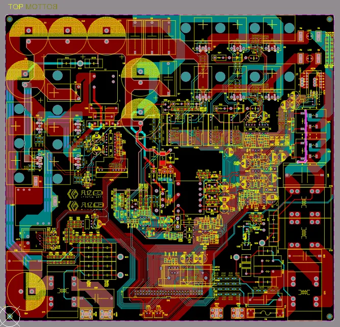
Millimeter-wave (mmWave) PCBs generally operate at frequencies such as 24 GHz, 28 GHz, 39 GHz, 60 GHz, 77 GHz, and 79 GHz, as well as even higher bands. Typical applications include 5G communications, satellite communications, ADAS automotive radar, high-speed AI interconnects, aerospace systems, and high-speed packaging modules.
From a manufacturing perspective, an mmWave PCB is not simply an upgraded version of a conventional high-frequency board. It combines microwave engineering, precision fabrication, materials science, and statistical process control. At these frequencies, electrical consistency is often more important than basic continuity and insulation performance.
Why Are Millimeter-Wave PCBs So Difficult to Design and Manufacture?
The fundamental challenge is the extremely short wavelength. At 1 GHz, the wavelength is approximately 300 mm. At 30 GHz, it is approximately 10 mm, while at 77 GHz it is only about 3.9 mm. As the wavelength becomes shorter, dimensional variations that would be negligible in a conventional PCB can produce measurable electrical effects.
Line-width variation, copper roughness, resin and glass-fiber distribution, lamination misregistration, hole-position error, surface finish, and glass-weave effects can all influence RF performance. These variations may appear as impedance discontinuities, phase shift, increased insertion loss, or degraded return loss.
For a conventional PCB, the primary requirements may be electrical continuity, insulation withstand, and long-term reliability. An mmWave PCB must additionally control impedance, phase, insertion loss, return loss, group delay, Dk and Df variation, conductor surface effects, and mode conversion. The complete signal path must be considered as an electromagnetic structure rather than merely as a set of connected copper features.

Typical Design Characteristics of mmWave PCBs
1. Very Low-Loss Materials
At millimeter-wave frequencies, dielectric loss and conductor loss become major contributors to attenuation. Materials are therefore selected for stable dielectric properties and low dissipation factor.
PTFE-based materials are commonly used in demanding RF applications. Examples include RO3003, RO4350B, and RT/duroid materials. Their typical advantages include low Df, stable Dk, and strong high-frequency performance. However, PTFE materials are soft, difficult to machine and drill, and more susceptible to dimensional instability caused by thermal expansion.
Hydrocarbon-ceramic materials, such as Megtron 6, Tachyon, and I-Speed, can be used in designs that combine high-speed digital and millimeter-wave sections. These materials can support mixed high-speed and RF constructions, although the suitability of a specific material depends on the stackup, frequency range, fabrication process, and required electrical performance.
2. Ultra-Low-Roughness Copper Foil
At high frequencies, the skin effect concentrates current near the conductor surface. At 30 GHz, the skin depth is only approximately 0.38 μm. If the copper roughness is around 2 μm, the roughness is several times greater than the depth in which most of the high-frequency current flows. From an electromagnetic perspective, the conductor surface is therefore extremely irregular relative to the current distribution.
This condition increases conductor loss and can raise insertion loss. For this reason, VLP, HVLP, ULP, and RTF copper foils may be considered for mmWave designs. Copper roughness must be controlled without compromising adhesion and other manufacturing requirements.
3. Fine Lines and Narrow Gaps
Millimeter-wave impedance is highly sensitive to trace width and the spacing between conductors. Typical line widths may be approximately 2–4 mil, with gaps of 2–3 mil. Some higher-frequency structures may require gaps below 2 mil.
These dimensions place stringent requirements on etching uniformity, undercut control, sidewall profile, and line-edge roughness. A trace can meet its nominal width during inspection while still producing unexpected RF behavior if its sidewalls or edges are excessively rough or asymmetric.
4. Highly Sensitive Transmission-Line Structures
Common mmWave transmission-line structures include microstrip, stripline, and coplanar waveguide with ground (CPWG). CPWG is widely used because it can provide stable impedance, convenient grounding, controlled radiation, and favorable EMI behavior.
However, CPWG fabrication is highly sensitive to the gap between the signal trace and adjacent ground conductors. Small dimensional errors change the electromagnetic field distribution and therefore shift the characteristic impedance. Even inspection errors at the AOI stage can become significant when the gap is only a few mils.

5. Very Thin Dielectric Layers
mmWave stackups may use 2 mil, 3 mil, or 4 mil core materials to achieve the required impedance geometry. Thin dielectric layers provide tighter electromagnetic control, but they are difficult to process. They can wrinkle, deform, or shift during handling and lamination.
Because dielectric thickness directly affects impedance, even a small change in the final pressed thickness can alter RF performance. Lamination control must therefore address material flow, thickness distribution, registration, and dimensional stability.
6. Specialized Via Structures
In an mmWave PCB, a via is not merely an electrical connection. It is part of the RF structure. Via stubs can behave as resonant structures and introduce reflection, insertion loss, and other discontinuities. Backdrilling is therefore often used to remove unnecessary via stubs.
Via fences may be placed alongside transmission lines to provide RF shielding and help constrain the electromagnetic field. Filled vias and VIPPO structures may also be used where the design requires a more continuous surface, reduced discontinuity, or improved control of mode conversion. The exact via configuration depends on the stackup and RF geometry.
7. Specialized Surface Finishes
Millimeter-wave designs are sensitive to conductor surface roughness and the electrical properties of surface-finish layers. ENIG may be unsuitable for some mmWave applications because the nickel layer can increase RF loss.
Depending on the application, alternatives may include immersion silver, immersion tin, ENPIG, or ENEPIG. Some designs may use a protected bare-copper surface. The selection must balance RF loss, solderability, corrosion resistance, assembly requirements, and long-term reliability.
Major Manufacturing Challenges
Material Machinability
PTFE does not behave like FR-4 during fabrication. It is soft, low in surface energy, resistant to moisture absorption, and difficult to bond. It can also deform during drilling. Typical problems may include smear, rough hole walls, nail heading, and resin recession.
PTFE Hole Metallization
PTFE is chemically inert, so conventional through-hole plating processes may provide insufficient adhesion. This can result in hole-wall separation, blistering, or poor reliability. Plasma treatment is commonly used to activate the surface and improve the conditions for subsequent metallization. This treatment is an important part of manufacturing PTFE-based RF boards.
Lamination of Mixed Materials
Many mmWave boards use hybrid constructions containing different materials, such as PTFE combined with FR-4. These materials can have different resin-flow behavior, thermal expansion, and dimensional shrinkage. As a result, lamination may produce warpage, layer shift, or delamination if the process window is not tightly controlled.
The lamination profile must be matched to the complete stackup. Temperature ramp rate, vacuum, pressure, gel time, and resin flow all influence the final dielectric thickness and registration. Because these parameters also affect impedance, lamination is part of the RF design process rather than an isolated mechanical operation.
Etching Accuracy and Copper Roughness
For mmWave circuits, etching quality must be evaluated by more than nominal line width. Line-edge roughness, undercut, sidewall profile, and conductor asymmetry can all affect high-frequency current distribution. A board may pass a conventional visual or AOI inspection while still failing an RF performance requirement.
Conductor roughness is a particularly difficult trade-off. Excessive roughness increases conductor-loss contribution to insertion loss. However, insufficient roughening can reduce bond strength and contribute to delamination or inadequate peel strength. The fabrication process must therefore balance electrical loss against mechanical adhesion and reliability.
Impedance Control
Typical impedance tolerances for conventional boards may be relatively broad, while high-speed boards often require tighter control. mmWave designs may require impedance tolerances of ±5% or, in some cases, ±3%. Achieving such control requires coordinated management of etch compensation, dimensional shrinkage, dielectric constant variation, copper thickness, and resin flow.
Impedance control is not determined by trace width alone. The complete geometry includes the conductor thickness, dielectric height, adjacent ground structures, material Dk, and the shape of the etched sidewalls. Any variation in these parameters can shift the impedance of the finished transmission line.
Glass-Weave Effect
Glass-weave effect becomes especially important at millimeter-wave frequencies because glass fibers and resin have significantly different dielectric constants. A representative glass-fiber Dk may be approximately 6, while the resin Dk may be approximately 2.3. As a trace passes over different proportions of glass and resin, its local electromagnetic environment changes.
This variation can produce local impedance nonuniformity, phase skew, and differential mismatch. To reduce the effect, designers and manufacturers may consider spread glass, flat glass, or finer glass weave constructions. The selected approach must be compatible with the required dielectric thickness and lamination process.
Key Production Controls for mmWave PCBs
1. Material Control
Dk and Df must be controlled for both batch-to-batch consistency and in-panel uniformity. A change in Dk can shift the electrical behavior of the transmission line and cause the finished structure to deviate from its intended frequency response. For this reason, a project may use controlled material lots, a fixed supplier, and a defined resin-content range.
2. Copper-Foil Roughness
Rz, Ra, and copper profile should be monitored rather than relying only on the nominal copper type. These parameters directly influence conductor loss and should be correlated with the actual RF construction.
3. Lamination Statistical Process Control
Temperature-rise rate, vacuum level, pressure profile, gel time, and resin flow require process monitoring. Thickness variation after lamination directly changes the transmission-line geometry and therefore the finished impedance.
4. Drilling Quality
Critical via structures require control of hole roughness, hole-position accuracy, smear, and wall condition. Manufacturing may use fresh drill bits, reduced hit counts, and optimized entry materials to improve hole quality. These controls are particularly important for PTFE and other soft RF materials.
5. Etching Capability
Etching control must address line-edge smoothness as well as finished width. Undercut, sidewall profile, and rough edges should be monitored because they influence the electromagnetic behavior of fine mmWave transmission lines.
Ultimately, mmWave PCB performance depends on the consistency of the entire fabrication chain. Materials, copper foil, lamination, drilling, plating, surface finish, and etching must work together as one controlled RF manufacturing process. Electrical continuity is only the starting point; stable impedance, low loss, repeatable phase behavior, and controlled electromagnetic geometry determine whether the finished PCB performs as intended.