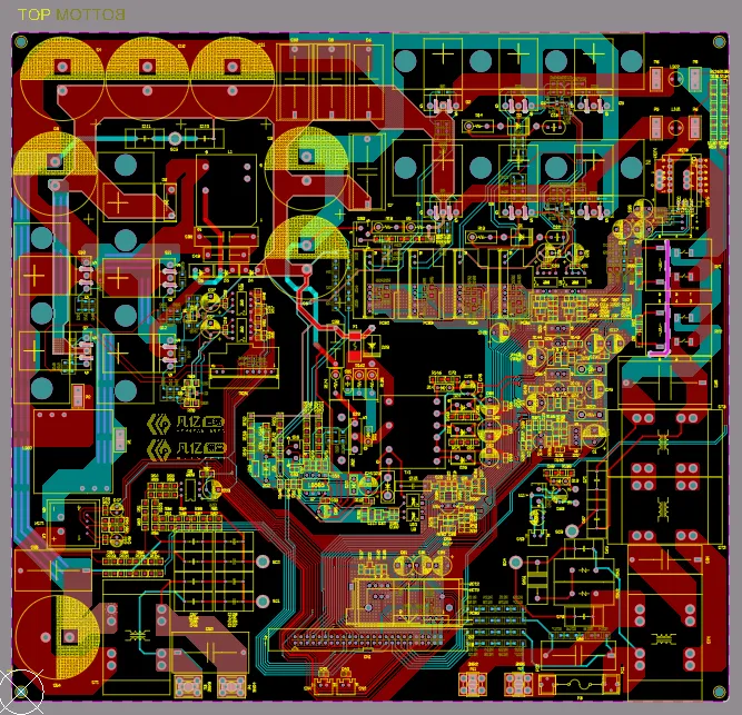
AI has been the dominant topic for several years.
What most people see are large models, compute chips, AI servers, and smart terminals. A more basic constraint is often ignored:
AI does not run on chips alone. It first has to run on a stable, efficient, and reliable power system.
- From data-center server power supplies to fast-charge adapters for AI terminals
- From digital power in industrial AI equipment to energy storage, photovoltaic systems, and EV chargers
- The higher the compute, power, and density, the more the product depends on a stable power system
Whether that power system can run safely, efficiently, and stably often comes down to PCB layout.
Talk of AI still starts with algorithms, chips, GPUs, and servers. In real hardware, long-term operation starts with power delivery.
- An AI server needs a stable power-conversion system
- An edge AI device needs reliable power management
- A high-power industrial controller must handle high voltage, high current, temperature rise, and EMC
- Energy storage, inverters, and charging equipment in new-energy applications need a complete high-power electronics design capability
The deeper the AI industry goes, the higher the demand on power electronics and power-PCB design.
AI is not a concept that stays in the cloud. It lands on circuit boards, power modules, and repeated, reliable power conversion. That is why power-PCB skill has become a capability hardware engineers cannot treat as optional.
Many engineers can lay out a conventional board and handle basic high-speed work. High-power boards are a different problem.
A high-power PCB is not a simple connectivity task. It is a system-engineering problem:
- Can the current pass safely?
- Is the copper current-carrying capacity enough?
- Do electrical clearance and creepage in the high-voltage area meet the requirement?
- Is the power-loop area under control?
- Have high dv/dt and high di/dt nodes been identified?
- Is the thermal path reasonable?
- Will EMI exceed the limit?
- Will layout details cause rework, board failure, or abnormal temperature rise in production?
Software commands do not answer those questions. A power PCB is not finished when the nets are connected. The system has to stay stable, safe, manufacturable, and producible under high voltage, high current, high temperature, and high interference. That is the hard part of AI's power foundation.
What makes a power-PCB layout engineer valuable is not dragging traces. It is making the right judgments, for example:
- Where is the main power loop?
- Where are the high-noise nodes?
- Where must traces be shortened?
- Where must copper be widened?
- Where is a via array needed for heat?
- Where must safety spacing be held strictly?
- Where should power ground, control ground, and digital ground be separated?
- Where should DFM, DFR, and EMC risk be considered early?
Those decisions determine whether a power board runs stably.
In topologies such as PFC, LLC, flyback, buck, boost, and inverters, layout affects efficiency and also temperature rise, noise, reliability, and certification risk.
For AI servers, power modules, industrial control, energy-storage inverters, and chargers, power-PCB design is no longer a single skill. It is the engineering link among circuit theory, device behavior, mechanical cooling, safety certification, and volume manufacturing.
High-power equipment raises the bar for layout engineers. The work is not limited to tool operation. It is the ability to design under high voltage, high current, high temperature, and high EMC risk.
That work typically covers:
- Common power topologies such as PFC, LLC, flyback, buck, boost, and inversion
- High-voltage / low-voltage partitioning and safety isolation
- Electrical clearance and creepage requirements
- Identification of high dv/dt and high di/dt nodes
- Power-loop area control
- Copper current-carrying calculations
- Via current-carrying assessment
- Multilayer stackup planning
- Power-ground, control-ground, and digital-ground treatment
- Protection of sensitive sense and feedback signals
- Thermal management and heat-path optimization
- Board-level EMC strategy
- DFM, DFR, and fabrication-file output
Those items sit behind AI server power, industrial AI equipment, and energy-storage, photovoltaic, and charging hardware. Once the design enters the high-power regime, they cannot be avoided.
The same issues appear across a wide power range, from small adapters to kilowatt-class equipment.
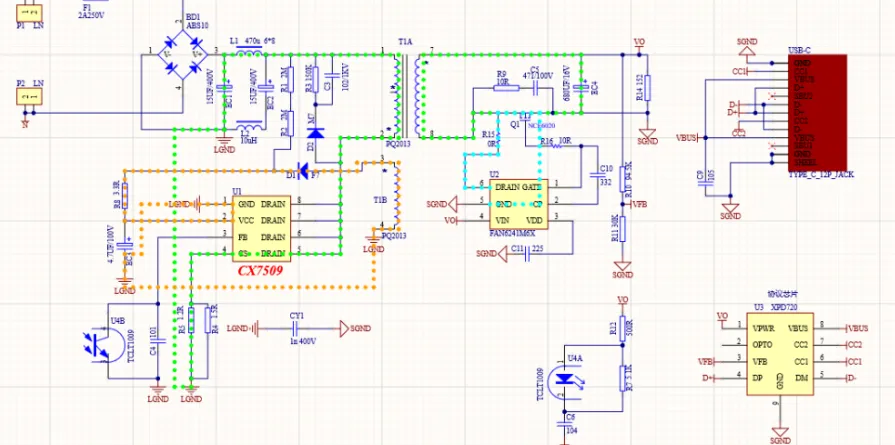
1. 20 W USB PD Adapter PCB
A flyback converter with a USB Type-C PD interface and synchronous rectification is a compact way to work through a production-level small adapter layout. It introduces safety rules, flyback topology, critical power loops, and EMI details.
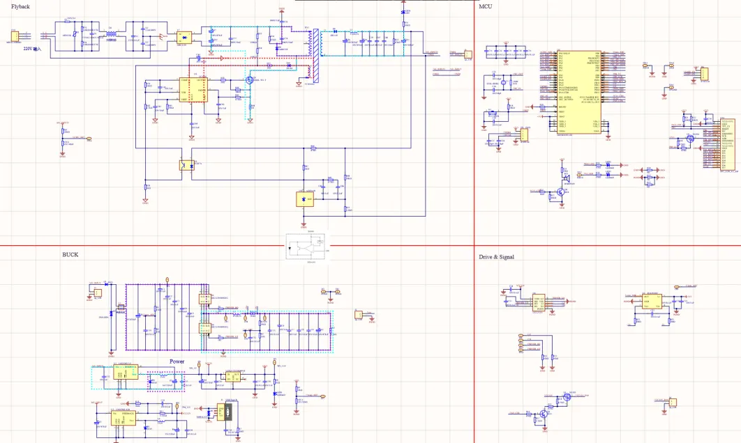
2. 90 W Adjustable Digital Buck Power PCB
Wide output voltage, high current adjustment, and high switching frequency force the layout to deal with conversion stages, buck step-down, split grounds, and sensitive-signal routing. The same problems show up in industrial equipment, consumer products, and other low- to mid-power supplies.
3. 460 W Interleaved CRM PFC plus LLC Industrial Power PCB
Interleaved CRM PFC, an LLC half-bridge resonant stage, and synchronous rectification are a common industrial-power structure. The layout work centers on EMI filtering, the PFC power loop, the LLC stage, high-voltage / low-voltage partitioning, multilayer stackup, copper current capacity, and via count. The same skills apply to server, telecom, and industrial supplies.
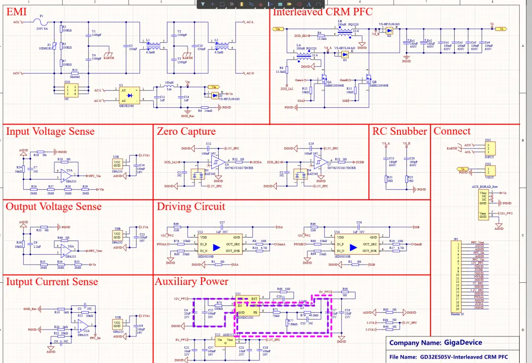
4. 500 W PFC plus LLC Industrial Digital Power PCB
A PFC plus half-bridge LLC topology brings PFC circuitry, the LLC half-bridge, voltage and current sensing, gate drive, OCP/OVP protection, multi-board interconnect, and power-ground versus control-ground treatment. That combination is typical of digital power, industrial supplies, and AI equipment power.
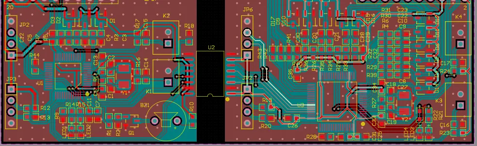
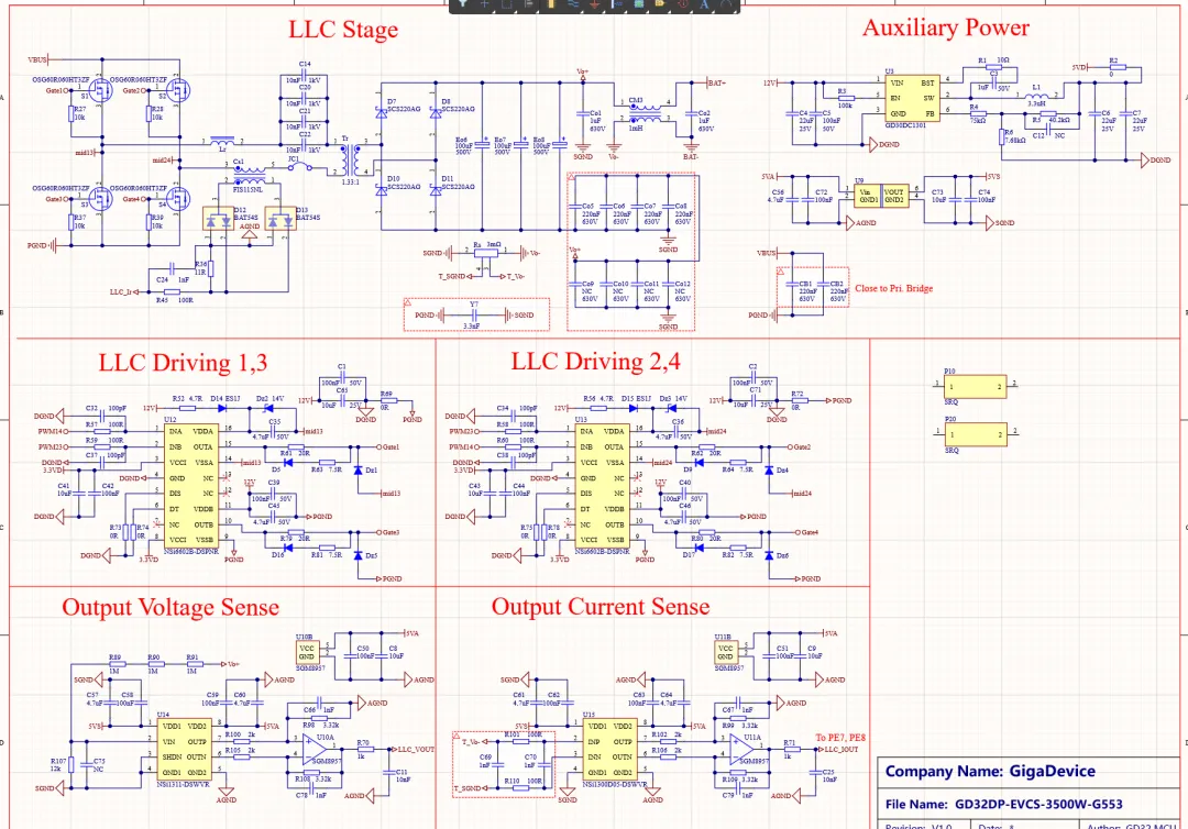
5. 3500 W DC Charging Power PCB
Totem-pole PFC plus full-bridge LLC is used on high-power boards for DC chargers and server supplies. The layout emphasis is totem-pole PFC, full-bridge LLC, high-voltage safety regions, control-circuit placement, high-voltage / low-voltage handling, power-loop identification, and EMI and thermal design at kilowatt level. System-level judgment matters more at this power.
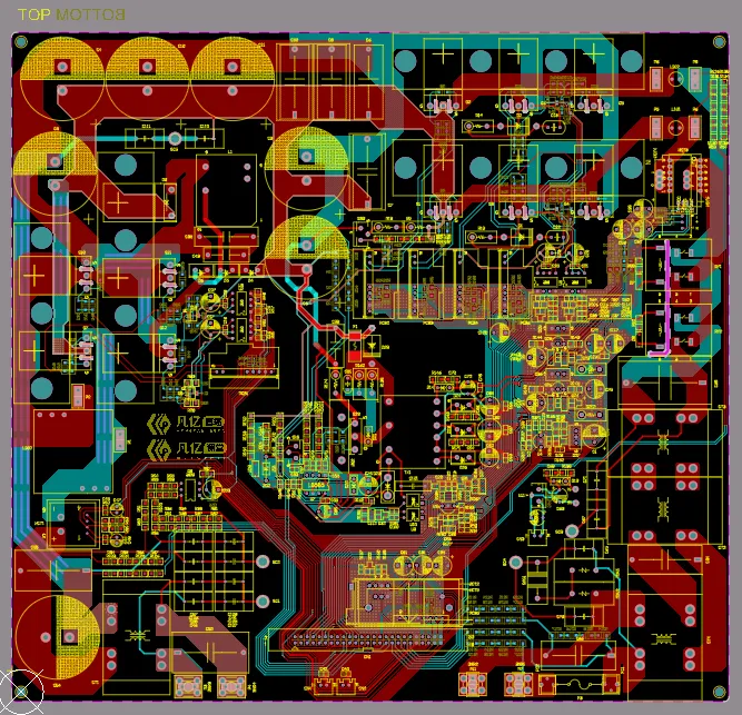
6. 3 kW Photovoltaic Inverter PCB
A 3 kW PV inverter main board typically combines boost and a single-phase full-bridge inverter. The layout work includes identifying dv/dt and di/dt hot spots, high-voltage / low-voltage design, copper current capacity, via-count calculation, thermal design, and DFM checks. Photovoltaic systems, energy storage, and inverters are part of the power infrastructure around AI-era compute.
Growth in AI will not create only algorithm and chip roles. It also increases demand for power engineers, hardware engineers, PCB layout engineers, and power-electronics engineers, because every high-compute product needs a more efficient, more reliable, higher-density power system.
That path is not limited to ordinary boards or basic tool operation. Higher-value work requires understanding:
- How power current should flow
- How heat should leave the board
- How noise should be controlled
- How safety rules should be kept
- How EMC risk should be reduced before layout is frozen
- How a design should move from schematic to volume production
That is the value of power-PCB design. It is not a niche skill. It is a central piece of the power foundation under AI hardware.
In practice, that means being able to plan a power-PCB stackup, design a high-current low-loss power path, control switching noise, protect sensitive sense loops, improve cooling, apply board-level EMC measures, and handle demanding applications such as PFC, LLC, multiphase buck, and SiC/GaN.
- In the AI era, compute matters.
- Stable compute depends on the power system.
- An efficient, reliable power system depends on power-PCB design.
What puts AI into hardware is not only the model in the cloud. It is also boards that keep converting power without failing.
AI ends at electricity. Electricity rests on engineering. Power-PCB design is a capability that engineering stack cannot ignore.
For engineers already doing PCB layout, hardware development, or power design — or moving toward new energy, industrial power, or AI server supplies — power PCB is the direction that stays scarce. The scarce skill is not operating the CAD tool. It is delivering projects that combine high voltage, high current, high temperature rise, and high EMC risk.