-
 00:49
00:49
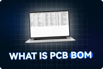
Why a "Simple" PCB BOM Causes So Many Project Problems
A PCB Bill of Materials (BOM) is a critical document that directly impacts component sourcing, assembly success, production timelines, and overall project cost. This video explains why incomplete or inaccurate BOMs can lead to procurement delays, incorrect component selection, manufacturing issues, and costly redesigns. It covers essential BOM requirements, including precise part numbers, package specifications, electrical characteristics, and approved component alternatives. The video also highlights practical strategies for managing supply chain risks, validating substitute parts, and aligning component choices with manufacturing capabilities. By implementing effective BOM management practices, engineers can improve procurement efficiency, reduce production risks, and ensure smoother PCB prototyping and mass production processes.
-
 00:54
00:54
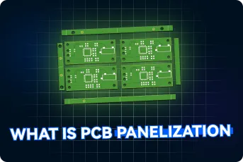
Why a Small PCB Can Cost More Than You Expect
PCB panelization is a key manufacturing technique that improves production efficiency by combining multiple circuit boards into a single panel for fabrication and assembly. This video explains how panelization reduces costs, increases throughput, and supports better manufacturing outcomes. It compares common depaneling methods, including V-cut and mouse bites, and outlines important design considerations such as routing clearance, tooling holes, fiducials, and assembly stability. By understanding proper panelization practices, engineers can improve yield, minimize damage during board separation, and optimize both prototype and volume production for FR4, multilayer, and high-reliability PCB applications.
-
 00:49
00:49
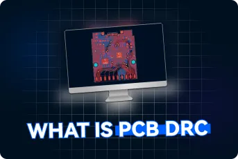
Why “Perfect” PCBs Fail in Production — DRC Explained
DRC (Design Rule Check) is a critical verification process that helps ensure a PCB design can be manufactured reliably and perform as intended. This video explains how DRC identifies potential issues such as trace spacing violations, insufficient annular rings, solder mask clearance problems, silkscreen conflicts, and component placement errors before production begins. It also explores how design complexity, board size, layer count, and via structures affect rule requirements. By properly reviewing and resolving DRC warnings and errors, engineers can prevent costly manufacturing defects, improve production yield, and enhance reliability in PCB prototypes and high-volume production projects alike.
-
 00:51
00:51
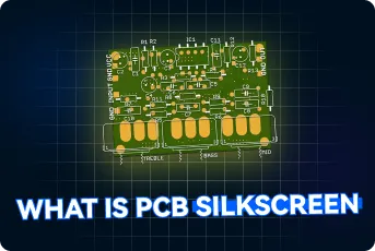
Why Silkscreen Still Matters
PCB silkscreen is a critical functional layer that supports accurate manufacturing, assembly, and inspection throughout the PCB production process. This video explains how silkscreen provides essential information such as component reference designators, polarity markings, and assembly instructions, while highlighting common design mistakes that can affect readability and production efficiency. It also covers key considerations including clearance requirements, line width, font size, board density, and fabrication tolerances. By following proper silkscreen design practices, engineers can reduce assembly errors, minimize rework, and improve manufacturing yield across rigid, flexible, and high-density PCB applications.
-
 00:57
00:57
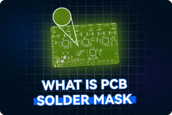
Solder Mask: The Layer That Quietly Prevents PCB Failures
Solder mask is a critical protective layer that plays a key role in PCB manufacturing quality, assembly yield, and long-term reliability. This video explains how solder mask controls solder flow, protects exposed copper, and helps prevent defects such as solder bridging and weak solder joints. It also covers essential design considerations, including pad openings, trace coverage, and via treatment options such as tented, plugged, and open vias. By understanding proper solder mask design rules and manufacturing tolerances, engineers can improve PCB performance, reliability, and production success across rigid, flexible, HDI, and multilayer PCB applications.
- Products & Service
- Company
- About AIVON
- Contact
- News
- Blog
- Certification
-


- Payment
-


2026 AIVON.COM All Rights Reserved