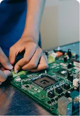
Why PCB Copper Pours Matter
# 4. WHAT THIS VIDEO COVERS
- This video explains the engineering purpose and practical implementation of copper pours on PCBs. It covers how properly connected copper areas create low-impedance ground paths that stabilize signals, simplify routing, and improve overall board performance. Viewers learn key thermal and mechanical benefits, as well as critical design rules such as avoiding excessive copper under pads and maintaining clearance from antennas to prevent soldering issues or RF detuning.
- The content compares strategies for 2-layer boards versus multilayer constructions, highlighting optimal ground placement for analog and digital circuits. Special attention is given to high-frequency designs where separate digital and analog ground pours are required. Real-world recommendations help engineers balance heat dissipation, noise reduction, and long-term maintainability.
The video is especially useful for teams working on 4 layer PCB(4 Layer PCB Board Service, Reliable Multi-Layer Fabrication | AIVON), high frequency PCB(High Frequency PCB Production, RF Material Fabrication | AIVON), and heavy copper PCB(Heavy Copper PCB Fabrication, High Current Board Service | AIVON) projects.
# 5. KEY HIGHLIGHTS
Copper pours tied to ground reduce impedance, stabilize signals, and improve thermal management in both 2-layer and multilayer PCBs.
Proper design avoids heat-sinking under pads and interference with antennas or RF circuits to maintain manufacturability and signal quality.
Multilayer boards require separate digital/analog pours, while 2-layer boards benefit from full bottom-layer ground planes for optimal performance.
# 6. FAQ
How do copper pours affect thermal performance in multilayer PCBs?
Copper pours act as large heat spreaders that lower thermal resistance and help dissipate heat from high-power components when properly tied to ground planes.
What are the recommended copper pour strategies for high-frequency PCB designs?
High-frequency designs require separate digital and analog copper pours to prevent ground loops, maintain signal integrity, and control impedance across different circuit sections.
How can improper copper pours impact signal integrity in automotive or industrial control applications?
Excessive copper under pads or near antennas can cause soldering defects, RF detuning, or increased noise, which reduces long-term reliability in automotive and industrial environments.
# 7. RELATED RESOURCES
Heavy Copper PCB(Heavy Copper PCB: Complete Guide to Design, Manufacturing, and High-Performance Applications)
High Frequency PCB(Copper Pour in Power Planes: Maximizing Current Capacity and Voltage Stability)
4 Layer PCB(Mastering PCB Copper Pour: Techniques for Effective Grounding and Noise Reduction)
PCB Assembly(PCB Turnkey Solutions & SMT Assembly Services)
Industrial Control PCB(Industrial Control PCB, Reliable Automation PCB Solutions | AIVON)
- Ever wondered what those large copper pours on a PCB actually do?
- Once tied to ground, they create a low-impedance path — stabilizing signals and simplifying routing. They help spread heat and even add mechanical strength.
- But copper pour needs care:
- Avoid full copper under pads — too much heat sinking can make rework harder.
- Keep it away from antennas — it can detune RF circuits or cause signal distortion.
Pouring strategies vary by board type:
For 2-layer boards: ground goes on the bottom, components and power lines on top.
For multilayer boards:
Analog circuits benefit from copper pour, but watch out for ground loop interference;
Digital circuits prefer large copper areas to reduce ground impedance and spike currents;
High-frequency designs require separate pours for digital and analog grounds to avoid sharing.
Copper pour is essential — but it needs balance between heat, noise, and maintainability.
This is aivon, making PCB learning easier,comment below — and follow for more PCB tips!