In today's high-power electronics landscape, Heavy Copper PCB technology has become indispensable. From electric vehicles and solar inverters to industrial motor drives and aerospace systems, devices demand circuit boards that can handle high currents, dissipate heat efficiently, and maintain reliability under extreme conditions. Standard PCBs with 1oz copper simply cannot meet these requirements.
This ultimate hub page serves as your comprehensive resource on Heavy Copper PCB. We will explore what heavy copper PCBs are, their significant advantages, critical design considerations, specialized manufacturing processes, and diverse real-world applications. You will also find practical guidance on overcoming challenges, selecting the right manufacturer, future trends, and answers to frequently asked questions.
Whether you are an electronics engineer, product designer, procurement specialist, or PCB enthusiast, this guide will equip you with actionable knowledge to leverage heavy copper technology effectively.
What Is a Heavy Copper PCB?
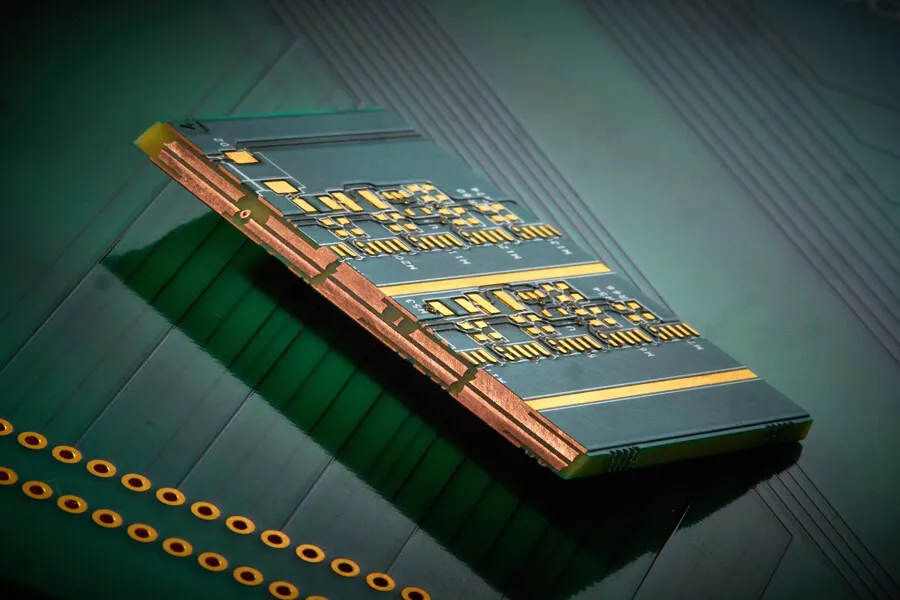
A Heavy Copper PCB, also known as a thick copper printed circuit board, is defined by its copper foil weight of 3 ounces per square foot (oz/ft²) or greater. In contrast, standard PCBs typically use 0.5oz to 2oz copper, while extreme copper PCBs can reach 20oz to 40oz or more for the most demanding applications.
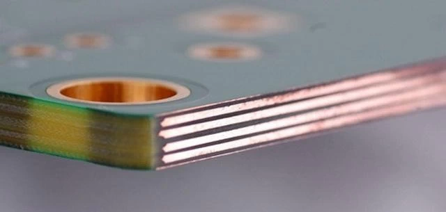
The copper thickness in a 1oz PCB is approximately 35 microns (1.37 mils). At 3oz, it jumps to about 105 microns, and at 6oz it reaches 210 microns. This increased thickness fundamentally changes the board’s electrical and thermal performance.
Heavy copper PCBs are usually built on FR-4, high-Tg FR-4, polyimide, or other substrates depending on the operating temperature and environment. They can be fabricated as rigid, flex, or rigid-flex boards. The technology follows IPC-6012 and IPC-2221 standards, which provide guidelines for minimum trace spacing, aspect ratios, and copper plating requirements.
Key Differences:
- Standard Copper PCB (1oz): Suitable for low-power signal boards.
- Heavy Copper PCB (3oz–10oz+): Designed for power distribution, heat sinking, and high-current paths.
- Extreme Copper PCB (20oz+): Used in military, rail traction, and very high-power industrial systems.
Heavy copper technology emerged from the need to replace bulky bus bars and external heatsinks with integrated solutions on the PCB itself. By embedding thick copper layers, designers can create planar transformers, high-current traces, and integrated heat spreaders in one board.
A cross-section of a heavy copper PCB typically shows trapezoidal trace profiles due to the etching process, substantial copper plating in vias (to ensure reliable current flow and thermal conductivity), and careful registration between layers to prevent misalignment on thick stacks.
This technology enables higher current-carrying capacity — a 10mm wide, 6oz trace can safely carry over 100 amperes with acceptable temperature rise — while significantly improving thermal management by conducting heat away from hot components more effectively than thin copper or thermal vias alone.
Key Benefits and Advantages of Heavy Copper PCBs
The shift to Heavy Copper PCB delivers numerous technical and economic advantages:
- Superior Current-Carrying Capacity — Thick traces reduce resistance and allow much higher current without excessive heating or voltage drop.
-
Exceptional Thermal Management — Copper is an outstanding thermal conductor. Heavy copper layers act as built-in heatsinks, spreading heat across the board or to attached heatsinks, often eliminating the need for external cooling solutions.
-
Enhanced Mechanical Strength — Thicker copper increases the board's structural integrity, making it more resistant to thermal cycling, vibration, and mechanical stress — critical for automotive, aerospace, and industrial applications.
-
Improved Reliability and Longevity — Better thermal performance reduces component stress and solder joint fatigue. Heavy copper boards often show superior performance in harsh environments (high temperature, humidity, vibration).
-
Reduced Layer Count and Board Size — High-current paths that would require multiple layers or external connectors in standard designs can be consolidated, lowering overall product cost and complexity.
-
Better EMI Performance — Wider, thicker power and ground planes provide lower impedance returns and improved shielding.
-
Cost Efficiency at Scale — Although material and processing costs are higher, heavy copper designs can reduce system-level costs by simplifying assembly, removing heatsinks, bus bars, and additional connectors.
Real-world data shows that a well-designed 4oz or 6oz board can reduce junction temperatures by 15–30°C compared to equivalent 1oz designs, dramatically extending component life. In renewable energy inverters, this can translate into higher efficiency and longer warranties.
Comparison Table: Standard PCB vs Heavy Copper PCB
| Feature | Standard PCB (1oz) | Heavy Copper PCB (≥3oz) |
|---|---|---|
| Current Capacity | Low–Medium | High (>100A possible) |
| Thermal Dissipation | Poor–Moderate | Excellent |
| Mechanical Strength | Standard | Superior |
| Typical Applications | Consumer, Signal | Power, Automotive, Industrial |
| Heat Sink Requirement | Often required | Often integrated |
| Layer Count Potential | Higher | Can be reduced |
These benefits make heavy copper technology the preferred choice when power density and reliability cannot be compromised.
Heavy-Copper PCB Design Principles, Rules, and Best Practices
Designing with heavy copper requires a different mindset than standard PCB layout. Trace width calculations must follow IPC-2221 formulas that account for current, temperature rise (typically targeting 10–20°C), and copper thickness. A 5oz trace can be significantly narrower than a 1oz trace while carrying the same current.
Key design considerations include:
- Proper thermal relief design for component pads
- Strategic placement of thermal vias (often filled and plated)
- Managing etching tolerances — thicker copper produces more pronounced trapezoidal traces
- Clearance and creepage distances for high-voltage applications
- Copper balancing to prevent warping during lamination
- Integration of copper coins or inlaid heatsinks for extreme thermal requirements
- Use of appropriate design software that accurately models thick copper
Component placement is critical — high-power devices should be positioned to take full advantage of thick copper planes for heat spreading. Power and ground planes should be maximized. Via structures often require “via farming” or larger diameters with heavy plating to ensure reliable current transition between layers.
For a complete, in-depth exploration of these topics including detailed formulas, design rules, simulation techniques, layout examples, and common pitfalls to avoid, read our specialized guide: Heavy-Copper PCB Design.
Heavy-Copper PCB Manufacturing: A Step-by-Step Guide
Manufacturing Heavy Copper PCB is considerably more complex than standard boards due to the challenges of etching thick copper, plating high-aspect-ratio holes, and managing material movement during lamination.
The process typically involves:
- Engineering and DFM review focused on copper balance and etch compensation
- Imaging with thicker photoresist or specialized dry film
- Controlled etching (often using step etching or compensated artwork) to achieve straight sidewalls
- Heavy copper plating for vias and through-holes (sometimes multiple plating cycles)
- Specialized lamination cycles with high-pressure presses and carefully selected prepreg
- Precision drilling and back-drilling
- Surface finishes such as ENIG, thick HASL, or OSP that are compatible with thick copper
- Rigorous quality control including cross-section analysis, thermal stress testing, and ionic cleanliness testing
Specialized techniques like “kiss etching,” resin-filled vias, and copper coin embedding are often employed. Registration accuracy becomes more challenging as copper thickness increases, requiring advanced equipment and experienced operators.
Our dedicated knowledge article provides a full Heavy-Copper PCB Manufacturing breakdown with diagrams, process parameters, and quality assurance methods: Heavy-Copper PCB Manufacturing.
Understanding these manufacturing realities during the design phase prevents costly revisions and ensures high yield.
Heavy-Copper PCB Applications: Powering High-Performance Electronics
Heavy Copper PCB Application spans any sector requiring robust power delivery and thermal performance.
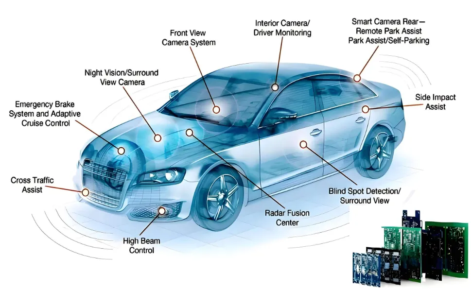
Automotive and Electric Vehicles: Battery management systems (BMS), on-board chargers, inverters, and motor controllers use heavy copper to handle hundreds of amps while operating in wide temperature ranges.
Renewable Energy: Solar inverters, wind power converters, and energy storage systems rely on thick copper boards for high-efficiency power conversion and long-term reliability.
Industrial Power Electronics: Motor drives, welding equipment, UPS systems, and industrial automation use heavy copper for its ability to survive continuous high-current operation.
Aerospace and Defense: Radar systems, avionics power supplies, and satellite equipment benefit from the technology’s mechanical strength and thermal performance in extreme environments.
Medical Equipment: MRI machines, X-ray generators, and surgical tools use heavy copper where failure is not an option.
Other growing areas include 5G base stations, data center power supplies, and robotics. In many cases, heavy copper enables miniaturization of high-power systems that were previously impossible.
For extensive case studies, sector-specific examples, and performance data, see our full article: Heavy-Copper PCB Application.
Challenges, Solutions, and Choosing the Right Manufacturer
Common challenges include higher material cost, etching undercut, layer registration, thermal stress during assembly, and limited availability of capable manufacturers. Modern solutions — advanced etching chemistry, laser drilling, filled vias, simulation-driven design, and experienced fabricators — have largely mitigated these issues.
When selecting a partner, look for proven experience with 4oz–12oz+ boards, strong DFM support, IPC Class 2 or 3 certification, thermal analysis capability, and transparent quality processes. AIVON specializes in heavy copper and extreme copper solutions with dedicated high-power production lines.
Future Trends in Heavy Copper PCB Technology
We are seeing growing adoption of embedded copper coins, hybrid heavy copper + flex designs, additive manufacturing techniques for copper, improved simulation tools using AI, and increasing demand for 10oz–20oz boards in electrification megatrends. Sustainability pressures are also driving optimization to reduce material usage while maintaining performance.
Conclusion
Heavy Copper PCB technology is a critical enabler for the next generation of high-power, high-reliability electronics. By understanding design principles, manufacturing realities, and application requirements, engineers can create products that are smaller, cooler, more efficient, and longer-lasting.
We encourage you to explore the linked sub-pillar pages for deeper knowledge and to contact the AIVON team for your next heavy copper project. Our engineers are ready to help turn your high-power requirements into reliable, high-performance circuit boards.
FAQs
Q1: What thickness is considered a Heavy Copper PCB?
A1: Heavy copper PCBs generally start at 3oz (approx. 105μm) copper thickness and commonly range from 4oz to 10oz, with some applications using 20oz or higher. Anything below 3oz is typically classified as standard or medium copper.
Q2: How much current can a Heavy Copper PCB carry?
A2: Current capacity depends on trace width, thickness, temperature rise allowance, and ambient temperature. A 6oz, 5mm-wide trace can often carry 50–80A with a 10–15°C temperature rise. Use IPC-2221 calculators or consult our Heavy-Copper PCB Design guide for precise values.
Q3: Is Heavy Copper PCB significantly more expensive?
A3: Material and processing costs are higher than standard PCBs, but total cost of ownership is often lower due to reduced need for additional heatsinks, connectors, bus bars, and fewer layers. The price premium decreases at higher volumes.
Q4: In which industries are Heavy Copper PCBs most commonly used?
A4: Key sectors include electric vehicles, renewable energy (solar/wind), industrial power conversion, aerospace/defense, medical imaging equipment, and telecommunications infrastructure.


