Introduction
Heavy copper PCB design has become essential for power electronics, electric vehicles, renewable energy systems, and industrial equipment. Unlike standard PCB design, heavy copper boards (typically 3oz or thicker) require specialized design principles to fully leverage their advantages in current handling, thermal performance, and long-term reliability.
This guide provides electrical engineers and PCB designers with actionable insights into heavy copper PCB design — from fundamental rules to advanced thermal and mechanical considerations. By understanding the heavy-copper PCB guide, designers can avoid common pitfalls and create boards that deliver both high performance and exceptional reliability.
Why Heavy Copper PCB Design Matters for Modern Electronics
Modern power systems are trending toward higher power density, compact form factors, and harsh operating environments. These demands push standard 1oz–2oz PCBs to their limits. Heavy copper PCB design addresses these challenges by enabling higher current capacity, better heat dissipation, and improved structural integrity.
When executed correctly, heavy copper designs can reduce layer count, eliminate external heatsinks, and significantly improve product lifespan. However, success depends on applying the right design principles from the very beginning.
Boosting Reliability: The Benefits of Heavy Copper PCBs
One of the strongest drivers for adopting heavy copper PCB design is the substantial improvement in product reliability.
Our comprehensive guide Boosting Reliability: The Benefits of Heavy Copper PCBs highlights several critical advantages:
- Improved thermal management and reliability — Heavy copper spreads heat more efficiently, reducing junction temperatures and thermal stress on components.
- Higher current capacity without failure — Thicker copper significantly lowers resistive losses, minimizing hotspots that cause premature aging.
- Reduced failure rates in demanding environments — Heavy copper boards exhibit superior performance under thermal cycling, vibration, and high-current continuous operation.
- Superior mechanical strength and vibration resistance — The thicker copper layers reinforce vias and pads, dramatically reducing the risk of cracking and trace delamination.
- Long-term reliability advantages of heavy copper — Many applications report 2–3x longer MTBF (Mean Time Between Failures) when properly designed with heavy copper.
These benefits of heavy copper PCBs make them particularly valuable in automotive, aerospace, renewable energy, and industrial control systems where failure is not an option.
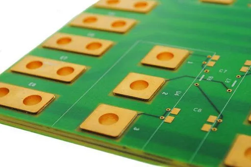
Critical Design Rules for Heavy Copper PCBs
Effective heavy copper PCB design begins with updated design rules. As copper weight increases, minimum trace width and spacing must expand to accommodate etching tolerances and plating buildup.
For 3oz copper, a typical minimum trace width is 0.25mm (10 mil), while 6oz designs often require 0.4–0.5mm or more. Copper distribution should be balanced across layers to prevent warpage during lamination.
Table 1: Heavy Copper vs Standard PCB Design Rules
| Design Parameter | Standard PCB (1–2oz) | Heavy Copper (3–6oz) | Design Impact |
|---|---|---|---|
| Minimum Trace Width | 0.15mm (6 mil) | 0.25–0.5mm | Affects current capacity and routing density |
| Minimum Spacing | 0.15mm | 0.25–0.4mm | Prevents shorts after plating |
| Via Aspect Ratio | 10:1 | 6:1 or lower | Critical for plating uniformity |
| Thermal Relief Spokes | 0.3mm width | 0.5–0.8mm width | Balances solderability and heat transfer |
| Copper Balance | Moderate | Critical | Prevents board warpage |
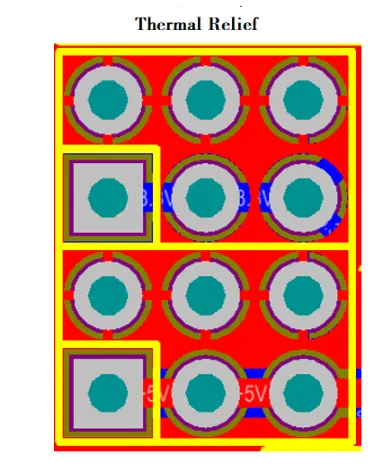
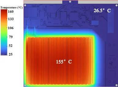
Thermal Management in Heavy Copper PCB Design
Thermal management is one of the biggest advantages in heavy copper PCB design. Thick copper acts as a heat spreader, moving heat away from hot components more effectively than standard designs.
Designers should implement thermal vias under high-power components, preferably filled and capped for maximum heat transfer. Copper pours on outer layers should be maximized while maintaining proper copper balance. High-Tg and low-CTE materials are strongly recommended to withstand the thermal stresses that heavy copper boards experience.
Current Carrying Capacity Design Guidelines
One of the primary reasons to adopt heavy copper PCB design is its superior current carrying capability. Using IPC-2221 and IPC-2152 standards, designers can accurately calculate trace width requirements based on temperature rise limits (typically 10–20°C).
For example, a 6oz trace that is 1.5mm wide can safely carry over 30A with only a 15°C temperature rise — performance impossible with standard 1oz copper without excessive width or external busbars.
When performing current carrying capacity calculations, always derate internal layers by approximately 50% due to reduced heat dissipation.
Table 2: Current Carrying Capacity Comparison (External Layer, 20°C Rise)
| Copper Weight | Trace Width | Current Capacity |
|---|---|---|
| 1oz | 2.5mm | ~8A |
| 3oz | 2.5mm | ~18A |
| 6oz | 2.5mm | ~28A |
| 10oz | 2.5mm | ~38A |
Via Design, Plating, and Aspect Ratio Considerations
In heavy copper PCB design, vias are critical thermal and electrical pathways. Aspect ratios should be kept below 6:1 (ideally 4:1) to ensure reliable plating.
Copper-filled vias or “via-in-pad” structures are frequently used under BGAs and power components. Back-drilling may be necessary in high-speed designs to reduce stub length. All vias should be properly sized to account for the additional plating thickness that accumulates during heavy copper processing.
Common Design Mistakes and How to Avoid Them
The most frequent mistakes in heavy copper PCB design include:
- Insufficient trace width and spacing leading to etching problems
- Poor copper balancing causing severe warpage
- Inadequate thermal relief design leading to soldering defects
- Overly aggressive aspect ratios resulting in plating voids
Working closely with your fabrication partner during the DFM (Design for Manufacturability) stage can prevent most of these issues.
Best Practices and DFM for Heavy Copper PCB Design
Successful heavy copper PCB design requires early collaboration with manufacturers. Provide clear stack-up drawings, copper weight specifications per layer, and acceptable temperature rise targets. Use symmetrical stack-ups and avoid abrupt transitions between heavy and fine features on the same layer when possible.
Always validate your design using thermal simulation tools and current capacity calculators before releasing for production.
Case Studies & Real-World Examples
A leading EV charger manufacturer redesigned a 400 A power module from 2 oz to 6 oz copper. By applying balanced copper distribution and filled thermal vias, they reduced board size by 35% and eliminated external heatsinks, cutting system cost by 22% while improving thermal cycling reliability by 3×.
In a solar inverter project, engineers increased copper weight from 1 oz to 4 oz on the outer layers of a 10-layer board. This change allowed them to handle 120 A continuous current on a single layer, reducing the total layer count from 12 to 8 and improving MTBF from 85,000 to 240,000 hours under 85 °C operating conditions.
Future Trends in Heavy Copper PCB Design
The next generation of heavy copper PCBs is moving toward extreme copper weights (10–20 oz) and hybrid constructions that combine heavy copper with embedded metal cores or thermal coins. Additive manufacturing techniques are enabling selective copper thickening, while AI-driven thermal simulation tools are becoming standard for optimizing current density in real time. By 2028, many high-power designs are expected to integrate 3D-printed copper structures directly into the PCB for even greater miniaturization and reliability.
Conclusion
Heavy copper PCB design requires a different mindset compared to standard PCB layout. When designers properly account for trace geometry, thermal pathways, via structures, and material behavior, the resulting boards offer exceptional electrical and mechanical performance. Applying the principles in this guide helps transform heavy copper from a difficult material into a powerful tool for creating reliable, high-performance electronic products.
FAQs
Q1: What copper thickness is considered heavy copper in PCB design?
A1: Heavy copper PCB design generally starts at 3 ounces per square foot. Thicknesses of 4oz to 10oz are common in high-current applications, while some extreme designs reach 20oz.
Q2: What via aspect ratio is recommended for heavy copper designs?
A2: A maximum aspect ratio of 6:1 is recommended, with 4:1 preferred for critical thermal or high-current vias to ensure reliable plating thickness on hole walls.
Q3: Does heavy copper PCB design require special layout software settings?
A4: While standard EDA tools can be used, custom design rules, adjusted clearance constraints, and copper balance checks are necessary. Many teams create dedicated heavy copper design templates.
Q4: When is it worth designing with heavy copper instead of standard copper?
A4: Heavy copper becomes advantageous when designs demand high current, strict thermal limits, improved mechanical robustness, or extended operating life under harsh conditions.


