In today's high-power electronics landscape, heavy copper PCB applications have become indispensable. Unlike standard PCBs with 1oz copper, heavy copper PCBs (typically 3oz to 20oz or more) deliver superior current-carrying capacity, exceptional thermal management, and enhanced mechanical strength. These characteristics make them the backbone of systems that demand reliable performance under extreme electrical and thermal loads.
From electric vehicle charging stations handling hundreds of kilowatts to precision robotics, aerospace avionics, and rugged industrial sensors, heavy copper technology enables designers to reduce layer count, minimize heat sinks, and improve overall product reliability. This sub-pillar page provides a complete overview of heavy copper PCB applications while linking to our in-depth cluster content for specific industry challenges and solutions.
Understanding Heavy Copper PCB Technology
Heavy copper PCBs are defined by copper weights exceeding 3oz per square foot, with many high-power designs using 4oz, 6oz, 10oz, or even 20oz copper. This increased copper volume fundamentally changes what a PCB can achieve:
- Current Capacity: A 6oz board can carry significantly more current than a 1oz board at the same temperature rise.
- Thermal Management: Copper acts as a heat spreader, reducing hot spots and eliminating or reducing external heatsinks.
- Mechanical Strength: Thicker copper improves connector durability and resistance to vibration and thermal cycling.
- Reduced Layer Count: Higher current capacity often allows designers to eliminate layers, lowering cost and improving reliability.
These advantages have driven the rapid adoption of heavy copper PCB applications across multiple high-demand sectors.
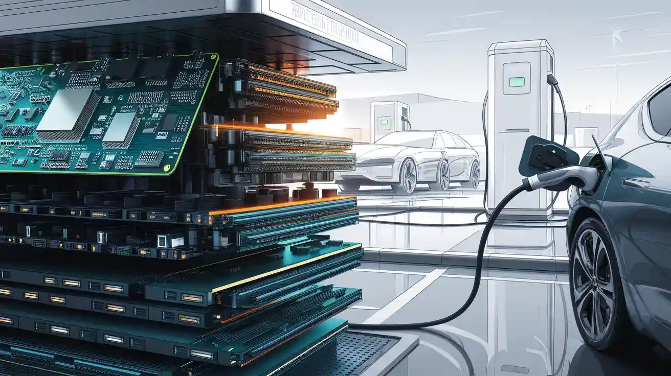
Heavy Copper PCBs for Electric Vehicle Charging Stations: Design Considerations
The global shift to electric mobility has created one of the most demanding heavy copper PCB applications today. DC fast chargers and ultra-fast charging stations must handle continuous high currents (often 200A–600A+) while maintaining safety and efficiency.
Key design considerations include optimized trace width and spacing for high amperage, strategic placement of thermal vias, copper pours for heat spreading, and material selection that can withstand constant thermal cycling. Proper design prevents voltage drop, minimizes heat generation, and ensures long-term reliability in 24/7 public charging environments.
For engineers working on next-generation chargers, our dedicated guideabout heavy copper PCBs for electric vehicle charging stations dives deep into thermal modeling, current distribution techniques, and UL safety compliance strategies specifically tailored for EV infrastructure.
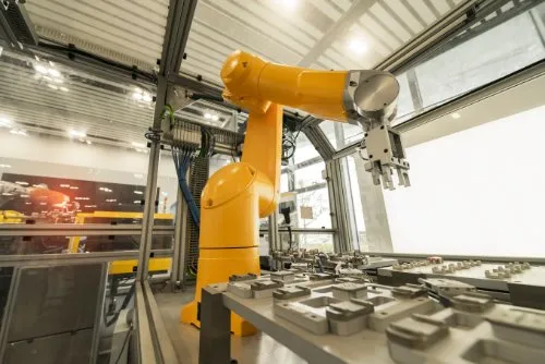
Heavy Copper PCB for Robotics: Boosting Your Robot's Performance
Modern robotics—whether industrial robotic arms, collaborative robots (cobots), or autonomous mobile robots—require compact, high-power motor drives, servo controllers, and power management systems. This is where heavy copper PCB for robotics delivers transformative results.
Thicker copper enables direct mounting of high-current components, superior heat dissipation from motor drivers, and improved electrical performance in compact spaces. The enhanced thermal conductivity also helps maintain precision and repeatability by reducing thermal drift in control circuits.
When designing motion control systems that demand both power and precision, heavy copper PCB for robotics becomes a game-changer. Our article about heavy copper PCB for robotics explores real-world implementations showing how 4oz–8oz copper designs improved torque consistency and reduced downtime in factory automation.
Heavy Copper PCBs Powering High-Demand Aircraft Cockpit Displays
Aerospace represents one of the most stringent heavy copper PCB applications. Aircraft cockpit displays must deliver brilliant visibility under direct sunlight while operating reliably across extreme temperature ranges (-55°C to +85°C and beyond) and intense vibration.
Heavy copper technology allows designers to power high-brightness LED backlights and complex processing electronics without adding excessive weight or external cooling systems. The thick copper layers also provide excellent electromagnetic shielding and improve overall board rigidity.
In aviation, where failure is not an option, heavy copper PCBs powering high-demand aircraft cockpit displays ensure both performance and reliability. Our specialized piece about heavy Copper PCBs for aircraft cockpit dsplays details how aerospace-grade designs meet DO-160 and MIL-STD requirements while managing extreme thermal loads.
Using Heavy Copper PCBs for High-Power Industrial Sensors
Industrial environments are among the harshest for electronics. High-power sensors used in predictive maintenance, process control, and heavy machinery monitoring must survive vibration, dust, chemicals, and significant electrical loads.
Using heavy copper PCBs for high-power industrial sensors provides the necessary current handling for powerful transducers while offering superior thermal dissipation to maintain measurement accuracy. The mechanical strength of thick copper also improves resistance to vibration-induced failures.
For applications requiring both precision sensing and rugged durability, using heavy copper PCBs for high-power industrial sensors has become an industry standard. Read our technical deep-dive guide about heavy copper PCBs for high-power industrial sensors to understand trace design strategies and long-term reliability testing protocols.

Additional High-Impact Heavy Copper PCB Applications
Beyond the four primary clusters above, heavy copper technology is expanding into:
- Renewable Energy: Solar inverters, wind power converters, and battery storage systems
- Medical Equipment: MRI machines, surgical robots, and high-power imaging systems
- Transportation: Rail systems, marine propulsion, and heavy-duty automotive powertrains
- Defense: Radar systems, electronic warfare equipment, and power supplies
Table: Heavy Copper PCB Applications Overview
| Industry | Typical Copper Thickness | Key Benefit | Primary Challenge | Related Cluster Content |
|---|---|---|---|---|
| EV Charging Stations | 6oz – 12oz | High current + thermal spreading | Continuous high-power cycling | Design Considerations |
| Robotics | 4oz – 8oz | Compact power + heat dissipation | Vibration & space constraints | Performance Boost |
| Aircraft Cockpit Displays | 4oz – 10oz | Reliability in extreme temps | Weight & DO-160 compliance | Aerospace Displays |
| Industrial Sensors | 4oz – 8oz | Accuracy in harsh environments | Vibration & contamination | High-Power Sensors |
| Renewable Energy | 6oz – 20oz | High efficiency power conversion | Thermal cycling | — |
Design and Manufacturing Considerations for Heavy Copper Applications
Successful heavy copper PCB applications require specialized design rules. Trace width calculators must be adjusted, copper balancing is critical to prevent warping, and specialized etching processes are necessary. Leading manufacturers use techniques such as step etching, embedded copper coins, and heavy copper plating to achieve optimal results.
Future Trends in Heavy Copper PCB Applications
The future of heavy copper PCB applications is evolving rapidly, driven by higher power densities, smarter designs, and sustainable manufacturing. Copper weights are expected to reach 20oz–40oz, enabling ultra-fast EV charging beyond 500kW and more powerful robotic systems.
Key trends include embedded copper coin technology, hybrid heavy copper with high-frequency materials, and AI-powered thermal optimization. In electric vehicles, heavy copper PCBs for electric vehicle charging stations will focus on extreme thermal management. The robotics sector will benefit from heavy copper PCB for robotics that deliver higher torque in smaller spaces. Aerospace and industrial applications will see greater adoption in aircraft cockpit displays and high-power industrial sensors, where reliability under harsh conditions remains critical.
Additionally, graphene-enhanced copper and 3D-printed heavy copper structures are emerging as game-changing solutions. These innovations will further expand the possibilities of heavy copper technology across high-power industries.
Conclusion
The rapid evolution of high-power electronics has firmly established heavy copper PCB applications as a cornerstone technology for industries demanding uncompromising performance, thermal management, and long-term reliability. From multi-hundred-ampere charging systems to precision motion control and mission-critical avionics, heavy copper PCBs deliver the electrical and mechanical integrity that standard boards simply cannot achieve.
At AIVON, we combine deep technical knowledge with advanced manufacturing capabilities to help customers unlock the full potential of heavy copper PCB applications. Whether you are developing next-generation EV infrastructure, high-performance robotic systems, aerospace electronics, or industrial sensing solutions, our team is ready to support your project from concept through volume production.


