Introduction
In railway signaling systems, printed circuit boards (PCBs) serve as the backbone for transmitting critical control signals that ensure safe train operations. Crosstalk, an unwanted electromagnetic coupling between adjacent traces, poses a significant threat to signal integrity in these high-reliability environments. Effective PCB layout techniques are essential to mitigate this issue, preventing data errors or timing failures that could compromise safety. Railway applications demand robust designs that withstand electromagnetic interference from power lines, motors, and track circuits while maintaining precise signal transmission. By focusing on proven layout strategies, engineers can enhance overall system performance and reliability. This article explores practical methods to minimize crosstalk through optimized PCB layout.
What Is Crosstalk and Why It Matters in Railway Signaling Systems
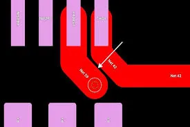
Crosstalk occurs when energy from an aggressor trace induces noise on a nearby victim trace through capacitive or inductive coupling. In PCB layouts, this phenomenon becomes prominent at higher frequencies or with closely spaced parallel traces, distorting the intended signal waveform. Forward crosstalk advances the victim's edge, while backward crosstalk delays it, both potentially violating setup or hold times in digital signals. In railway signaling systems, where timing accuracy is paramount for interlocking and train detection, even minor crosstalk can lead to false triggers or communication failures. Signal integrity directly impacts safety-critical functions, making crosstalk minimization a non-negotiable aspect of design. Compliance with standards like IEC 61508 for functional safety further underscores the need for interference-free PCB layouts.
Fundamental Mechanisms of Crosstalk in PCBs
Capacitive crosstalk arises from electric field coupling between traces, proportional to their overlapping area and inversely related to separation distance. Inductive crosstalk stems from mutual inductance when current changes in the aggressor create magnetic fields that link to the victim trace. Both effects intensify with longer parallel runs and faster signal rise times common in modern railway control systems. Impedance discontinuities, such as unmatched trace widths or vias, exacerbate coupling by reflecting signals that reinforce noise. Understanding these mechanisms allows engineers to target layout parameters systematically. Ground bounce and power supply noise can also amplify crosstalk, highlighting the interconnected nature of PCB parasitics.
PCB Layout Techniques for Optimizing Trace Routing and Spacing
Maintaining adequate spacing between traces is one of the most straightforward ways to reduce capacitive coupling strength. Engineers should minimize parallel trace lengths, routing signals perpendicularly where possible to limit overlap. Increasing separation distance exponentially decreases field coupling, providing a first-order mitigation. For high-speed signals, controlled impedance routing ensures consistent propagation, reducing reflections that worsen crosstalk. Route sensitive signals away from high-swing outputs or clocks to avoid aggressor-victim interactions. These practices form the foundation of crosstalk-resistant PCB layouts.
Leveraging Ground Planes and Shielding Techniques
Solid ground planes adjacent to signal layers act as shields, absorbing stray fields and providing low-impedance return paths. Placing a ground plane directly beneath or above signal traces confines electromagnetic fields, significantly attenuating broadside coupling between layers. Shielding techniques, such as stitching vias along trace edges, create Faraday cage-like barriers that divert noise currents. In multilayer boards, alternating signal and ground planes in the stackup enhances isolation. Ground planes also stabilize reference planes for impedance control, indirectly supporting signal integrity. These methods prove particularly effective in noisy railway environments.
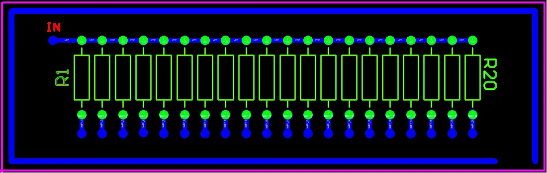
Implementing Differential Pair Routing
Differential signaling pairs transmit data as complementary signals, inherently rejecting common-mode noise including crosstalk. Layout requires tight coupling between pair traces with consistent spacing to ground, typically achieved via length-matched routing. Avoid splitting pairs across layers or introducing asymmetries that unbalance coupling. Differential routing excels in railway applications for serial links used in communication protocols. Terminate pairs properly to prevent reflections that could couple to nearby singles. This technique boosts noise immunity while preserving signal quality.
Layer Stackup Strategies for Crosstalk Reduction
Strategic layer stackups position signal layers between ground planes to minimize inter-layer coupling. Avoid stacking sensitive signals directly adjacent without shielding; instead, use ground-signal-ground configurations. Orthogonal routing on facing layers reduces edge coupling from aligned traces. Thicker dielectrics between signal layers further weaken fields. For railway PCBs, balanced stackups support thermal management alongside EMI control. Simulate stackup effects early to validate isolation performance.
Incorporating Guard Traces and Additional Shielding
Guard traces, grounded and placed between victim signals, intercept coupling fields before they reach adjacent lines. Connect guards frequently with vias to the nearest ground plane for effective shunting. This method suits dense layouts where full spacing is impractical. In combination with shielding cans or enclosures for the entire board, guards provide multi-level protection against external EMI common in railway signaling. Regularly space stitching vias along high-risk interfaces to form continuous shields. These passive elements enhance robustness without active components.
Railway-Specific Considerations in PCB Layout
Railway signaling systems operate in harsh conditions with vibration, temperature extremes, and high EMI levels from traction systems. Layouts must prioritize mechanical stability, using wider traces and anchor points to resist flexing that could alter spacings. Integrate robust power distribution networks isolated from signals via dedicated planes. Adhere to IPC-2221 guidelines for trace clearances and layer sequencing to ensure reliability. Signal integrity verification through pre-layout simulations catches issues early. These tailored approaches align with the high-stakes demands of railway applications.
Best Practices for Implementation and Verification
Begin with schematic reviews to flag potential aggressors, then apply constraints in the layout tool for automated spacing enforcement. Perform post-layout signal integrity analysis to quantify crosstalk levels and iterate designs. Fabricate prototypes for empirical testing under simulated railway conditions. Collaborate across teams for design rule checks aligned with IPC-6012 performance specs. Document layout decisions for traceability in safety certification processes. Continuous refinement ensures optimal crosstalk performance.
Conclusion
Minimizing crosstalk in PCB layouts for railway signaling systems requires a holistic approach combining spacing, shielding, and stackup optimization. These techniques preserve signal integrity, safeguarding critical operations against interference. Ground planes, differential routing, and guard traces emerge as core strategies, adaptable to multilayer complexities. Railway engineers benefit from standards-guided practices that balance performance and reliability. Implementing these methods proactively reduces risks and enhances system longevity. Prioritizing layout excellence ultimately supports safer rail transport.
FAQs
Q1: What is crosstalk in PCB layout for railway applications?
A1: Crosstalk refers to unintended signal coupling between PCB traces, degrading signal integrity through capacitive or inductive mechanisms. In railway signaling, it can distort timing-critical data, risking operational errors. Mitigation involves spacing traces adequately and using ground planes as shields. Following structured layout rules prevents most issues.
Q2: How do shielding techniques improve signal integrity in high-reliability PCBs?
A2: Shielding techniques employ ground planes and vias to confine electromagnetic fields, blocking crosstalk between traces. Adjacent ground layers absorb noise, while stitching creates barriers. In railway systems, this counters external EMI effectively. Consistent application maintains waveform fidelity across frequencies.
Q3: Why is PCB layout critical for minimizing crosstalk in signaling systems?
A3: PCB layout dictates coupling proximity and field containment, directly influencing crosstalk levels. Poor routing amplifies noise in parallel high-speed traces. Optimized designs with perpendicular paths and guards ensure clean signals. For railways, this upholds safety by preventing false detections.
Q4: What role do layer stackups play in crosstalk reduction?
A4: Layer stackups isolate signals via interleaved ground planes, minimizing broadside coupling. Orthogonal orientations on adjacent layers further limit interactions. Balanced dielectrics enhance isolation. Engineers tailor stackups for railway EMI resilience, verifying through analysis.
References
IPC-2221B — Generic Standard on the Design of Rigid Printed Boards. IPC, 2012
IPC-6012E — Qualification and Performance Specification for Rigid Printed Boards. IPC, 2017
IEC 61508 — Functional safety of electrical/electronic/programmable electronic safety-related systems. IEC, 2010


