-
 00:54
00:54
What are Antipads in PCBs?
Antipads are critical clearance areas in copper planes that prevent unwanted electrical connections between vias and power or ground layers in multilayer PCBs. This video explains how antipads work, why they are essential for signal integrity, and how their size affects parasitic capacitance, impedance control, and crosstalk. It also highlights the role of proper antipad design in improving power distribution, return current paths, and overall PCB reliability. These considerations are especially important in 4-layer, multilayer, HDI, and high-frequency PCB designs used in IoT, industrial, automotive, and aerospace applications.
-
 00:57
00:57
What is an Annular Ring in PCB?
The annular ring is a critical PCB design feature that directly impacts manufacturing yield and long-term reliability. This video explains the importance of proper annular ring sizing, the risks of drill misalignment and breakout, and IPC-recommended design guidelines. It also introduces practical solutions such as teardrops to improve pad integrity and maintain electrical connections. These best practices are essential for ensuring reliable vias and robust performance in FR4 PCBs, HDI PCBs, and multilayer circuit boards used in demanding applications.
-
 00:53
00:53
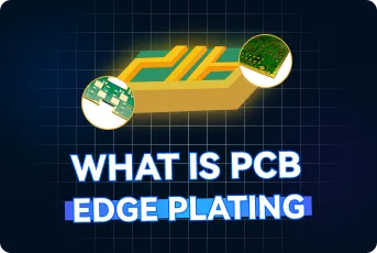
What Is Edge Plating? The PCB Trick You’ve Probably Seen
This video explains PCB edge plating, a specialized fabrication process that deposits copper along the edges of a circuit board to create electrical and mechanical connections between layers. It covers the key benefits of edge plating, including improved ground continuity, reduced EMI, enhanced heat dissipation, and increased mechanical durability. The guide also discusses important design considerations, manufacturing requirements, and cost implications associated with this advanced PCB feature. Commonly used in RF systems, high-frequency PCBs, aerospace equipment, medical devices, and industrial electronics, edge plating can significantly improve performance and reliability when properly implemented.
-
 00:47
00:47
Why PCB Stack-up Design Matters More Than You Think
This video explores the importance of PCB stack-up design and how proper layer arrangement influences signal integrity, power distribution, EMI performance, and overall board reliability. It explains best practices such as placing signal layers next to ground planes, optimizing power-to-ground plane spacing, and selecting suitable prepreg structures to maintain impedance control. Using common 4-layer and multilayer PCB configurations as examples, the guide demonstrates how effective stack-up planning helps reduce noise, crosstalk, and power instability. These principles are essential for PCB prototypes and high-performance designs used in high-frequency, automotive, medical, and industrial electronic applications.
-
 00:46
00:46
What Is PCB Stack-up? Understanding Layers and Prepregs Explained!
This video explains the fundamentals of PCB stack-up and its importance in PCB design, fabrication, and performance. Using a 4-layer PCB as an example, it demonstrates how copper layers and dielectric materials are laminated together, with a focus on the role of prepreg in bonding layers, controlling thickness, and supporting impedance requirements. The guide highlights how stack-up decisions influence signal integrity, thermal performance, mechanical stability, and manufacturing reliability. Ideal for engineers working on PCB prototypes, multilayer PCBs, RF designs, automotive electronics, and medical devices, this video provides practical insights into selecting the right materials and layer configurations for successful PCB production.
- Products & Service
- Company
- About AIVON
- Contact
- News
- Blog
- Certification
-


- Payment
-


2026 AIVON.COM All Rights Reserved