










PCB Specifications
| Parameter | Value | Parameter | Value |
|---|---|---|---|
| PCB Type | FR4 PCB | Quantity | 5 pcs |
| Layers | 4 Layers | Board Type | Panel PCB |
| Dimensions | 158.4 x 87.8 mm | Copper Weight | 1oz |
| Thickness | 1 mm | Min Track / Spacing | 5/5mil |
| Surface Finish | ENIG (Immersion Gold) | Min Hole Size | 0.2mm |
| Solder Mask | Green | Silkscreen | White |
| Stack-up | Default | Impedance Control | No |
Manufacturing Timeline
Logistics Information
Key Manufacturing Processes
Manufacturing Summary
This 4-layer FR-4 PCB was produced in a quantity of 40 pieces at 1.0 mm finished thickness using TG150 material with 1 oz copper on all layers. Board dimensions measured 158.4 × 87.8 mm in a 4×2 panel arrangement, featuring 5 mil minimum line width and spacing, ENIG surface finish, green solder mask, and white silkscreen. Mechanical routing combined with V-scoring was applied, and 100% flying probe testing verified electrical continuity within the 3-day lead time.
Several DFM items required clarification before production release. Trace-to-outline clearances fell short of standard requirements (routing edge ≥0.2 mm, V-cut edge ≥0.4 mm), prompting a 0.1 mm outward shift of the V-cut and outline that was confirmed acceptable after dimensional comparison. Multiple silkscreen characters overlaid pads and were adjusted by removing text from pad areas to prevent soldering defects. IC pad open-window connections were retained per original design, model marking placement across solder mask and silkscreen layers was verified, and indicated positions were confirmed as MARK points corresponding to 1.5 mm holes.
Edge clearance and silkscreen adjustments were implemented after customer confirmation, ensuring reliable depanelization and clean solderability. Production maintained consistent registration and surface finish quality across the batch. Detailed records of the edge clearance and V-cut adjustment method applied to this order provide further reference for similar tight-geometry multilayer boards.
Explore More PCB Manufacturing Resources
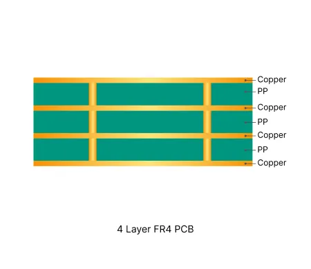
4 Layer FR4 PCB Manufacturing Insights
Discover how AIVON manufactures 4 Layer FR4 PCBs, including multilayer stackup design, layer alignment control, fabrication processes, manufacturing challenges, and real production experience from customer orders.

How to Avoid Common Engineering Queries in Multilayer FR4 PCB Design
Real multilayer FR4 PCB CAM review cases covering stack-up confirmation, impedance control, copper balance, via tenting, and edge clearance EQs. Discover practical DFM best practices for 4-layer and higher boards to reduce engineering queries, prevent warpage, and improve first-pass yield.
Real Production Records
| Order ID | PCB Type | Layers | Dimensions | Solder Mask | Surface Finish | Quantity | Action |
|---|---|---|---|---|---|---|---|
| FR4-20260911-001 | FR4 PCB | 4 | 76.33 x 49.91 | Green | HASL Lead Free | 10 | View detail |
| FR4-20260819-043 | FR4 PCB | 10 | 157 x 140 | Blue | ENIG (Immersion Gold) | 100 | View detail |
| FR4-20260818-014 | FR4 PCB | 2 | 110.32 x 173.3 | Green | ENIG (Immersion Gold) | 200 | View detail |


