Coupons
Help
  • FAQ
    browse most common questions
  • Live Chat
    talk with our online service
  • Email
    contact your dedicated sales:
EN
EN

Engineering Cases

Engineering Cases focuses on real PCB engineering reviews, manufacturing challenges, and production optimization processes from actual fabrication projects. This category highlights how different PCB designs are evaluated and adjusted during engineering review, covering topics such as stack-up analysis, impedance control, drill optimization, copper balancing, solder mask alignment, DFM review, and production risk assessment across various PCB applications. The content in this section is based on practical manufacturing scenarios rather than theoretical introductions. Each engineering case demonstrates how specific PCB issues are identified, analyzed, and resolved during production preparation and fabrication. These records help engineers, purchasers, and hardware teams better understand the relationship between PCB design decisions and manufacturing stability, yield control, and process reliability. Topics may include multilayer PCB engineering review, HDI process optimization, flexible PCB manufacturing considerations, heavy copper processing adjustments, surface finish selection, Gerber data verification, and other real-world PCB production experiences. By organizing engineering challenges and process solutions into structured case content, this category provides valuable insight into practical PCB manufacturing and engineering workflow management.

 
How to Prevent Solder Mask Bridge Failure and NSMD BGA Issues in 8-Layer PCB
PCB Panelization HDI PCB Design For Manufacturing Multilayer PCB Design Solder Mask Troubleshooting Via Plugging Solder Bridging BGA Assembly

How to Prevent Solder Mask Bridge Failure and NSMD BGA Issues in 8-Layer PCB

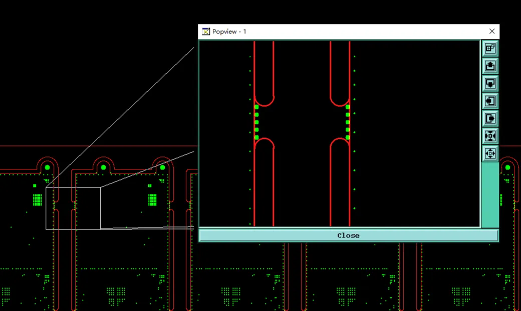
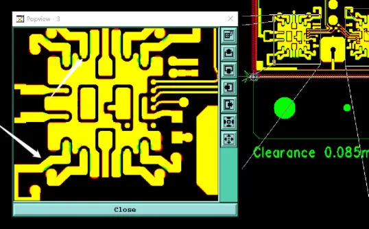
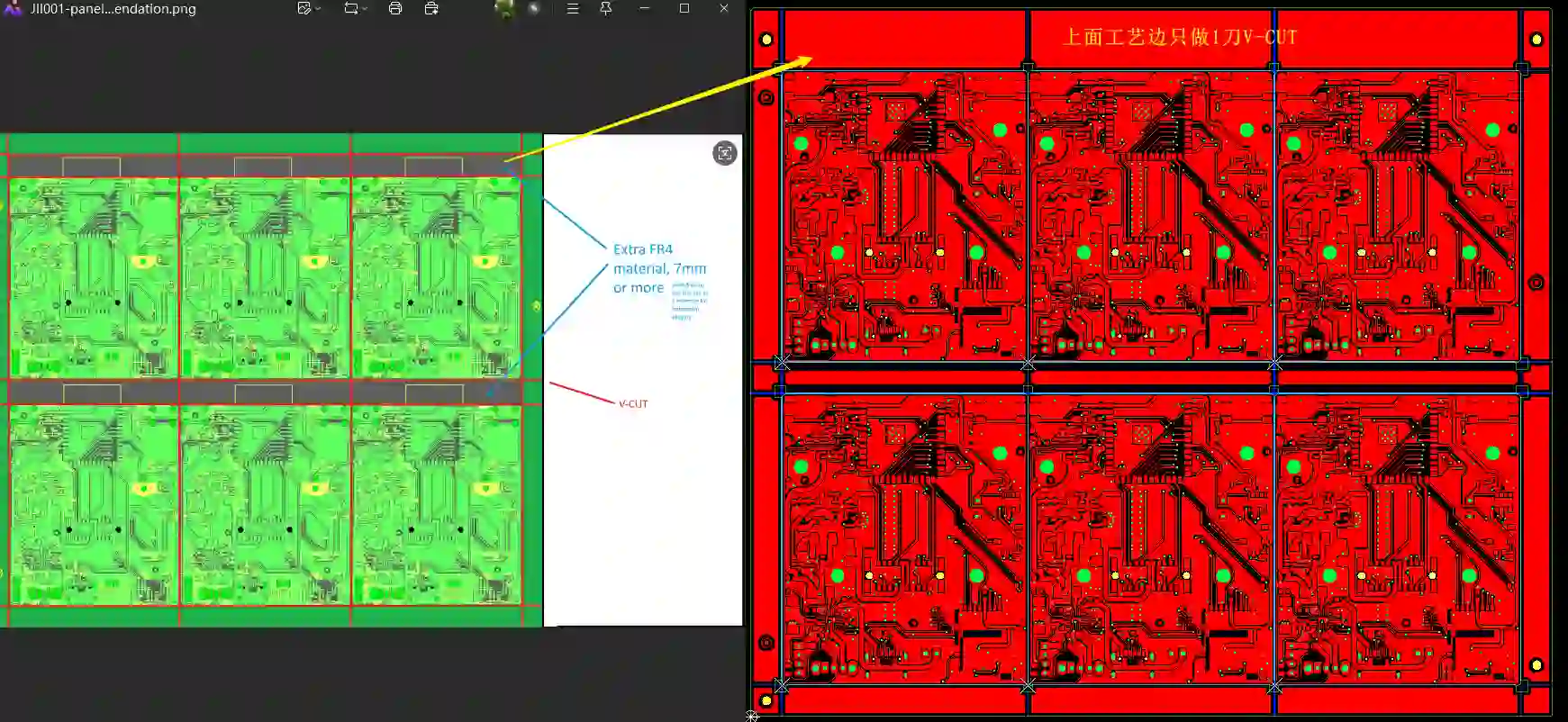
Real 8-layer 1.0mm FR-4 PCB CAM review case with tight SMD pad spacing causing solder mask bridge failures, NSMD BGA risks, via mask conflicts, and panelization optimization. Discover DFM solutions for ENIG finish, stackup, and stamp holes to reduce EQs and improve assembly yield.

How to Resolve Backdrill, Press-Fit & Copper Balance Issues in 3mm 24-Layer FR4 PCB
PCB Warpage Copper Balancing Via Stubs Design For Manufacturing High-Temperature PCB Via Plugging PCB Back Drilling

How to Resolve Backdrill, Press-Fit & Copper Balance Issues in 3mm 24-Layer FR4 PCB

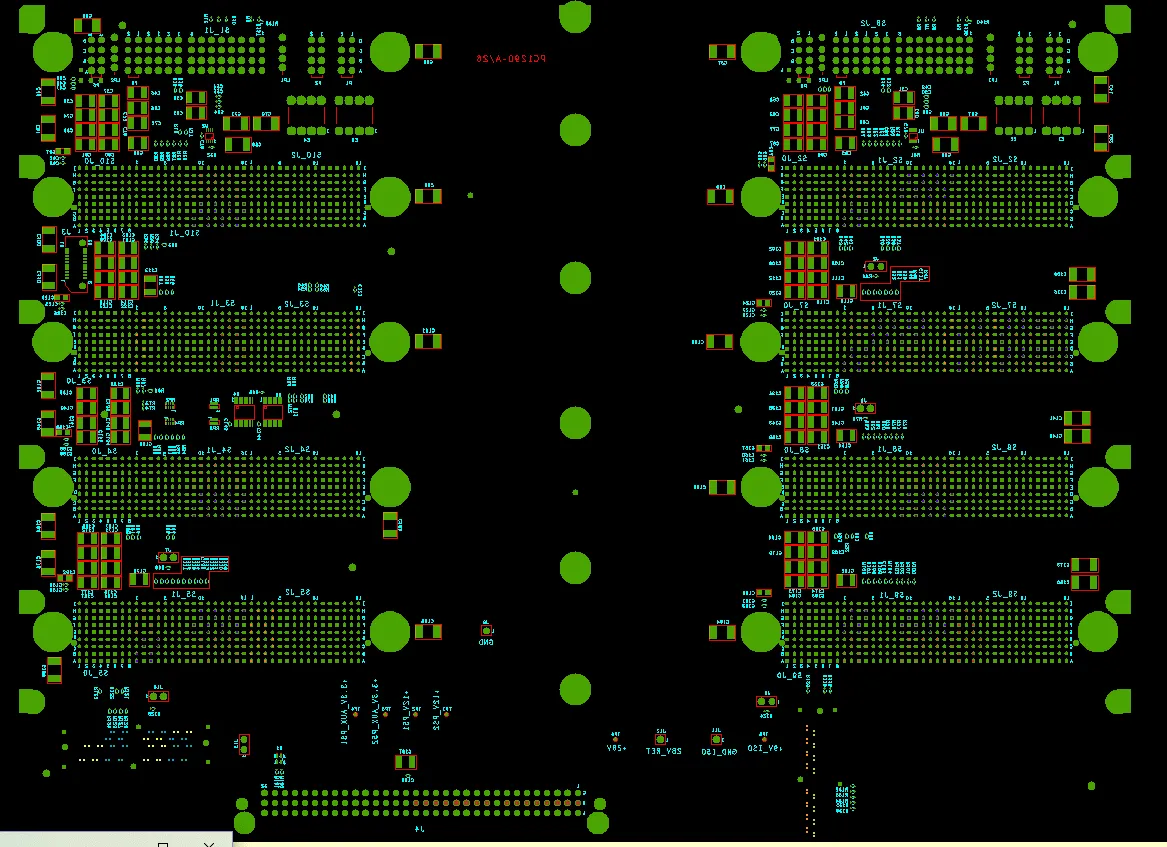
Discover how our CAM team handled over 20 EQs on a 3mm 24-layer FR4 PCB, including tight backdrill stubs, press-fit hole tolerances, via plugging conflicts, and warpage risks. This engineering case details practical DFM solutions for high-reliability thick multilayer boards to prevent scrap and ensure signal integrity.

Fixing 18-Layer PCB Risks: The Power of PCB CAM Review
PCB Manufacturing Defects Impedance Control Copper Balancing Design For Manufacturing PCB Back Drilling PCB Stackup Design PCB Lamination High-Tg Fr4

Fixing 18-Layer PCB Risks: The Power of PCB CAM Review

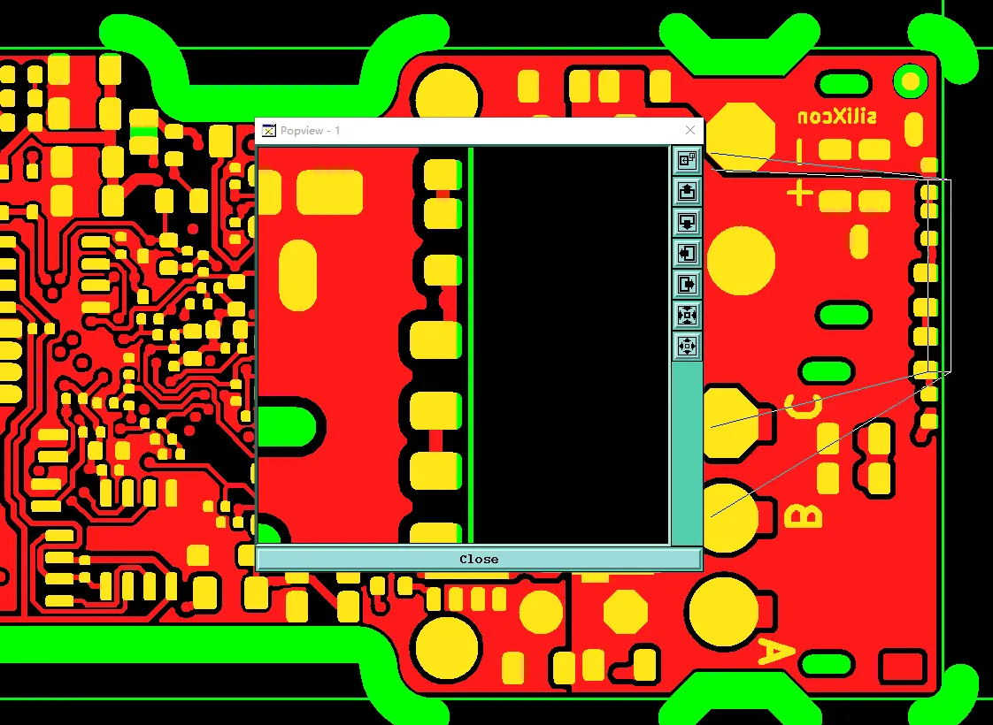
Explore a real 18-layer FR-4 TG170 PCB CAM review EQ case with impedance stackup, copper-free areas causing lamination risks, back drilling, and resin-plugged via mask conflicts. Learn practical DFM solutions for material substitution, copper balancing, and markings to prevent yield loss and ensure signal integrity in high-reliability boards.

How to Avoid Countersink & Copper Issues in 3mm Thick FR4 PCB Manufacturing
PCB Copper Weight PCB Drilling PCB Mechanical Design PCB Warpage Design For Manufacturing High-Temperature PCB Copper Thickness PCB Stackup Design

How to Avoid Countersink & Copper Issues in 3mm Thick FR4 PCB Manufacturing

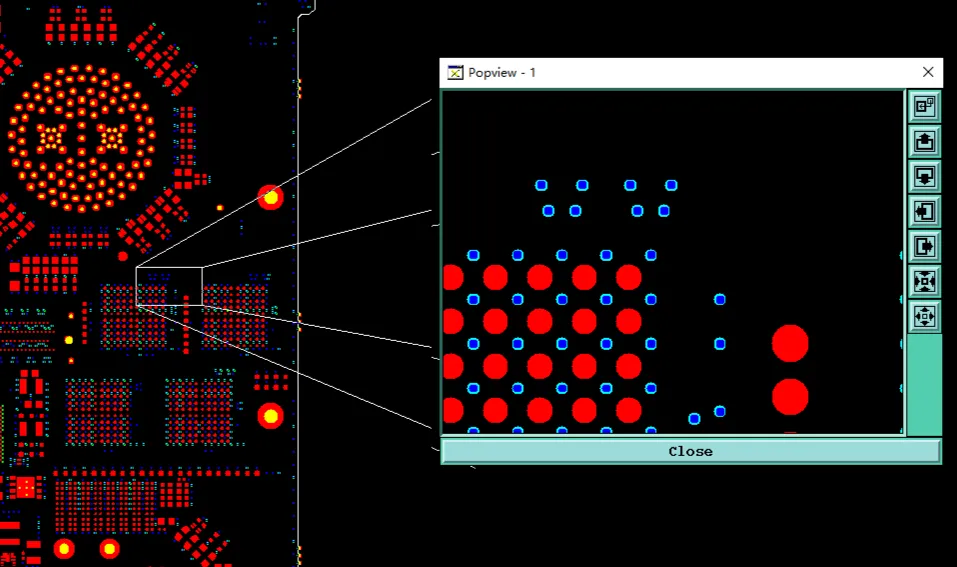
Learn how our CAM team resolved countersink dimension mismatches, copper thickness conflicts, and D-hole clearance problems on a 3mm thick FR4 PCB. This real engineering case shows critical DFM checks for precision countersink holes in FR4 PCB to prevent assembly failures and ensure reliable production.

How We Resolved Stackup Warpage, Blind Via Spacing & No-Mask Conflicts in Hybrid Rogers RF PCB
PCB Materials Signal Integrity Blind Vias High-Frequency PCB PCB Stackup Design For Manufacturing RF PCB Design Substrate Warpage

How We Resolved Stackup Warpage, Blind Via Spacing & No-Mask Conflicts in Hybrid Rogers RF PCB

In this real PCB CAM review for a 4-layer hybrid Rogers RF PCB (RO4003C + RO4350B), we addressed critical issues including stackup asymmetry causing warpage risk, tight trace space violations, blind via spacing, V-CUT clearance, and solder mask conflicts. Learn practical DFM solutions that ensured successful fabrication and signal integrity.

Engineering Challenges in 2 Layer Aluminum PCB Manufacturing: DFM and Thermal Issues
Thermal Management Copper Balancing Design For Manufacturing PCB Thermal Performance PCB Delamination PCB Stackup Design Thermal Via Stitching

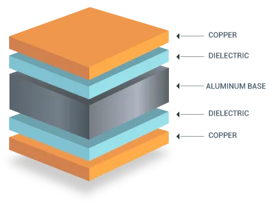
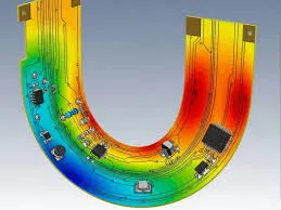
Engineering Challenges in 2 Layer Aluminum PCB Manufacturing: DFM and Thermal Issues

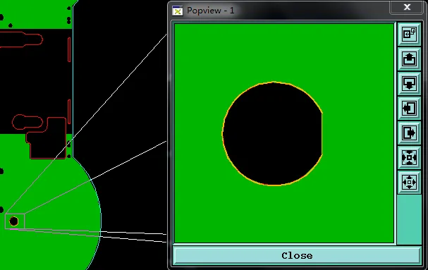
Explore common engineering queries in 2 layer aluminum PCB manufacturing, including CTE mismatch, thermal via design, dielectric bonding, and solder mask registration issues. Learn practical DFM solutions to reduce warpage, improve thermal performance, and increase production yield.

Why Extra Long Aluminum PCBs Trigger EQs: Common DFM Issues & Fixes
PCB Panelization Thermal Management Solder Mask Misalignment Design For Manufacturing MCPCB Defects High Current PCB

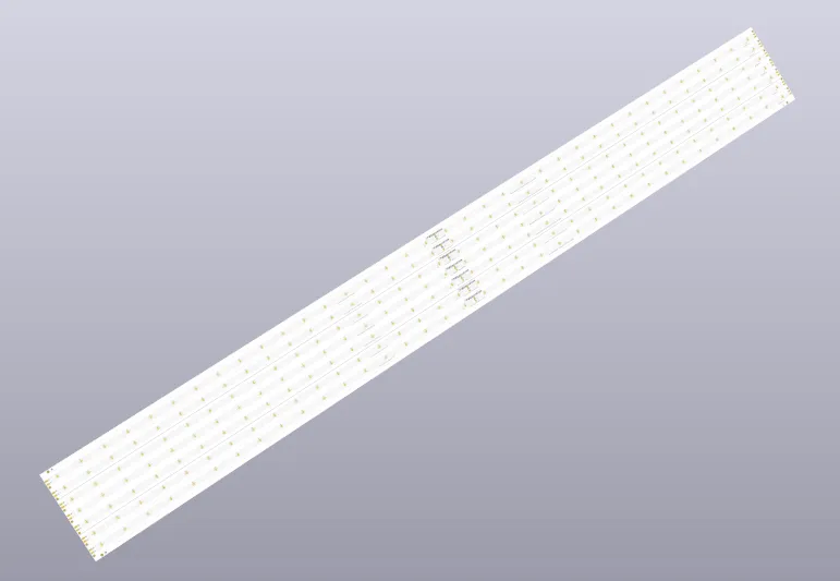
Why Extra Long Aluminum PCBs Trigger EQs: Common DFM Issues & Fixes

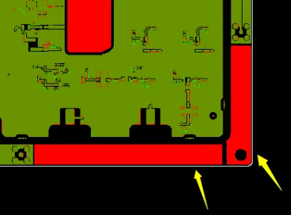
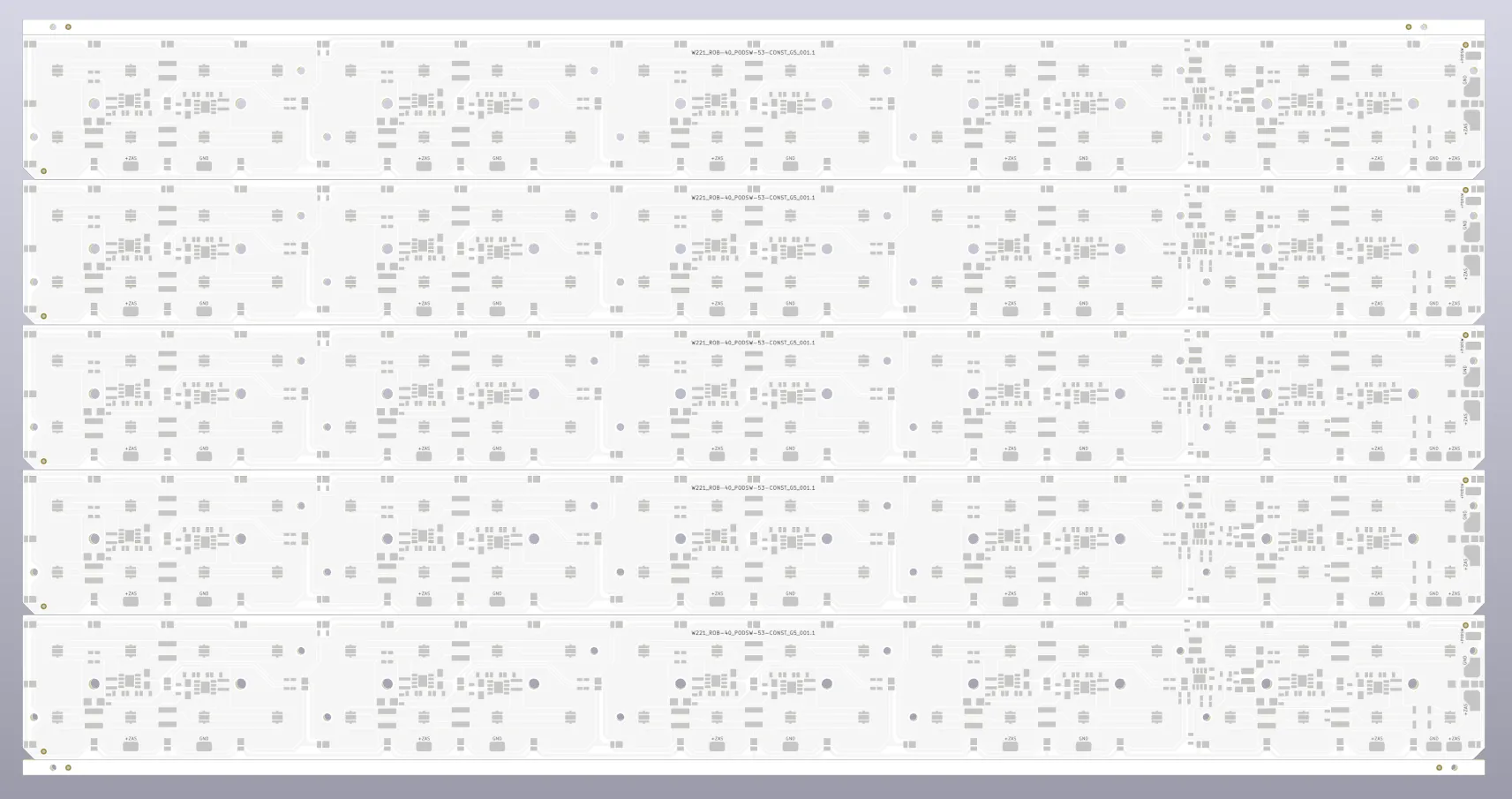
Explore the top causes of Engineering Queries (EQs) for extra long aluminum PCBs, including thermal via placement, copper balance, solder mask registration, and panelization challenges. This real-world engineering case shares practical DFM best practices to prevent warpage, plating defects, and production delays in LED and power applications.


2026 AIVON.COM All Rights Reserved
Intellectual Property Rights | Terms of Service | Privacy Policy | Refund Policy