Introduction
Manufacturing 2-layer flexible PCBs requires more than just standard rigid-board expertise. The transition to polyimide substrates and double-sided copper layers introduces critical variables in mechanical stress management, registration, and surface protection. Engineering Queries (EQs) are a common hurdle in this process, often signaling potential failures in dynamic bending or assembly. By understanding why these queries occur—ranging from improper bend radius definitions to coverlay misalignment—you can proactively optimize your DFM strategy. This guide outlines the most frequent EQ triggers in double-sided flex production and provides expert-backed best practices to streamline your CAM review, reduce lead times, and ensure the long-term reliability of your flex circuits.
The Role of Engineering Queries in 2-Layer Flex Reliability
Engineering Queries, or EQs, are formal requests from the fabrication team for clarification or correction when design files contain ambiguities, conflicts, or potential manufacturability risks. For 2 layer flexible PCBs, these queries are particularly common because the material properties and dynamic mechanical requirements differ significantly from standard rigid boards. In the factory, unresolved issues during file review can lead to scrapped panels, extended lead times, or reliability failures in the field. Clear communication at the EQ stage ensures that the final product meets both electrical and mechanical expectations without costly iterations.
Common 2-Layer Flex Design Pitfalls and DFM Issues
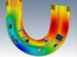
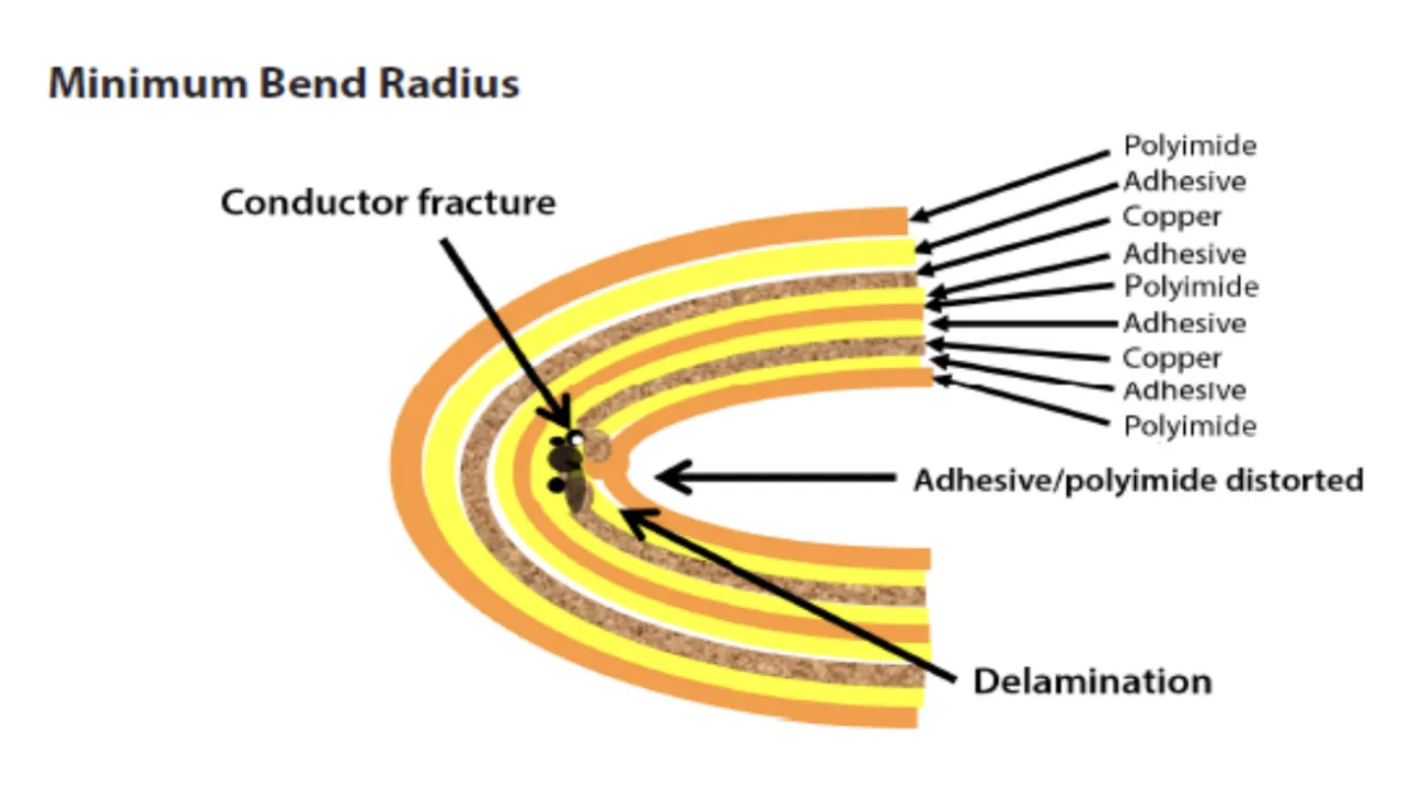
One frequent issue involves insufficient or unspecified bend radius in the flex zone. Designers often provide tight curves without indicating whether the application is static or dynamic, or they omit the expected number of flex cycles. This happens because bend requirements are sometimes assumed from rigid board experience rather than calculated based on the total thickness of the 2 layer construction including coverlay. During engineering review, the DFM software flags potential trace cracking risk, and the team sends an EQ asking for confirmation of the minimum inside bend radius and bend type. If not clarified, the board may suffer copper fatigue or cracking after limited bends, resulting in open circuits and field failures.
Another common query concerns coverlay window sizing, alignment, and transition to any rigid areas or stiffeners. In double-sided flex designs, coverlay must precisely expose component pads while protecting traces, yet adhesive flow or misalignment during lamination can cover pads or create exposed copper risks. The root cause is often missing or conflicting coverlay Gerber files, or lack of clear callouts for selective application. CAM engineers detect this through overlay checks and registration simulations, prompting an EQ for confirmation of coverlay type, adhesive thickness, and exact window dimensions. Without resolution, the result can be coverlay encroachment, leading to poor solderability or short circuits during assembly.
Plated through-hole reliability in 2 layer flex also triggers many clarifications, particularly regarding via placement relative to bend areas and plating thickness. Designers sometimes place vias too close to dynamic flex zones or specify hole sizes without considering the higher aspect ratio challenges on thin flex material. This stems from applying rigid board via rules directly to flex. In DFM review, the system highlights risks of barrel cracking due to flexing stress, generating an EQ for via-to-bend distance, stagger requirements, or confirmation of minimum plating thickness. Unaddressed, vias can develop cracks over time, causing intermittent electrical opens and reduced product lifespan.
Copper balance and trace routing symmetry between the two layers frequently appear in EQs as well. Uneven copper distribution or stacked traces on opposite sides can cause warpage or uneven bending behavior in the finished board. The cause is often asymmetrical artwork or failure to mirror traces for neutral axis placement. Engineering review identifies this via copper density calculations and stack-up analysis, requesting clarification on intended copper weight per layer and any requirements for balanced construction. If ignored, the board may warp during lamination or exhibit inconsistent flexibility, affecting both assembly and long-term reliability.
Why CAM Reviewers Flag 2-Layer Flexible Designs
During the initial CAM and DFM analysis of 2 layer flexible PCB files, engineers compare the provided Gerbers, drill files, and stack-up notes against factory process capabilities for polyimide-based materials. Ambiguities arise because flex designs involve additional layers such as coverlay and stiffeners that rigid boards do not require, yet these are sometimes incompletely documented. Factory teams also simulate bending stress and lamination flow, which reveal issues not apparent in standard EDA checks. The thin substrate and plated holes introduce tighter process windows for registration and etching, making even small deviations significant. These factors combined lead to proactive EQs aimed at preventing defects before production begins.
Proactive DFM Strategies to Streamline 2-Layer Flex Production
To reduce engineering queries, clearly specify the bend radius, bend type (static or dynamic), and expected cycle count directly in the fabrication drawing or readme file. Indicate the neutral bend axis and avoid placing vias or wide traces within the bend zone where possible. For coverlay, provide dedicated Gerber files with precise windows and include notes on adhesive type and any selective application requirements. Use teardrop pads at vias and maintain adequate annular ring sizes to accommodate flex-specific etch factors. Balanced copper distribution and symmetrical routing between layers help minimize warpage; consult with the manufacturer early for recommended copper weights in 2 layer constructions. Finally, include a detailed stack-up diagram showing all materials, thicknesses, and tolerances to align expectations before production.
Conclusion
2 layer flexible PCBs offer excellent solutions for compact and dynamic applications, yet their manufacturability depends heavily on addressing flex-specific details during the design phase. In factory experience, most engineering queries stem from incomplete documentation around bending, coverlay, and via placement rather than fundamental electrical errors. By incorporating clear callouts, following material-appropriate guidelines, and engaging with the fabrication partner early, designers can significantly reduce EQ volume and achieve smoother production runs. This proactive approach not only shortens lead times but also enhances the mechanical reliability of the finished boards in their intended environments.
FAQs
Q1: What is the typical minimum bend radius for a 2 layer flexible PCB?
A1: For double-sided flex circuits, the minimum inside bend radius is generally calculated based on the total build thickness, often around 10 to 12 times the thickness for static applications. Dynamic flexing requires more conservative values to avoid copper fatigue and cracking. Final values should always be confirmed with material stack-up and cycle requirements.
Q2: Why do 2 layer flex designs need separate coverlay Gerber files?
A2: Coverlay is a laminated protective film instead of liquid solder mask, so it requires precise window definitions for pad exposure. Separate Gerbers ensure accurate alignment and prevent misregistration that could block pads or expose traces unintentionally.
Q3: Can vias be placed in the bend area of a 2 layer flexible PCB?
A3: It is strongly discouraged to place vias in dynamic bend regions because repeated flexing can cause barrel cracking. If unavoidable, they must be kept outside the bend radius or carefully staggered with sufficient mechanical clearance.
Q4: How does copper balance affect flexible PCB reliability?
A4: Uneven copper distribution can cause uneven stress during bending and lamination, leading to warpage or inconsistent flexibility. Balanced routing helps maintain mechanical stability and improves long term reliability.
References
IPC-2223E — Sectional Design Standard for Flexible Printed Boards. IPC, 2020
IPC-6013D — Qualification and Performance Specification for Flexible Printed Boards. IPC, 2019
IPC-A-600H — Acceptability of Printed Boards. IPC, 2020