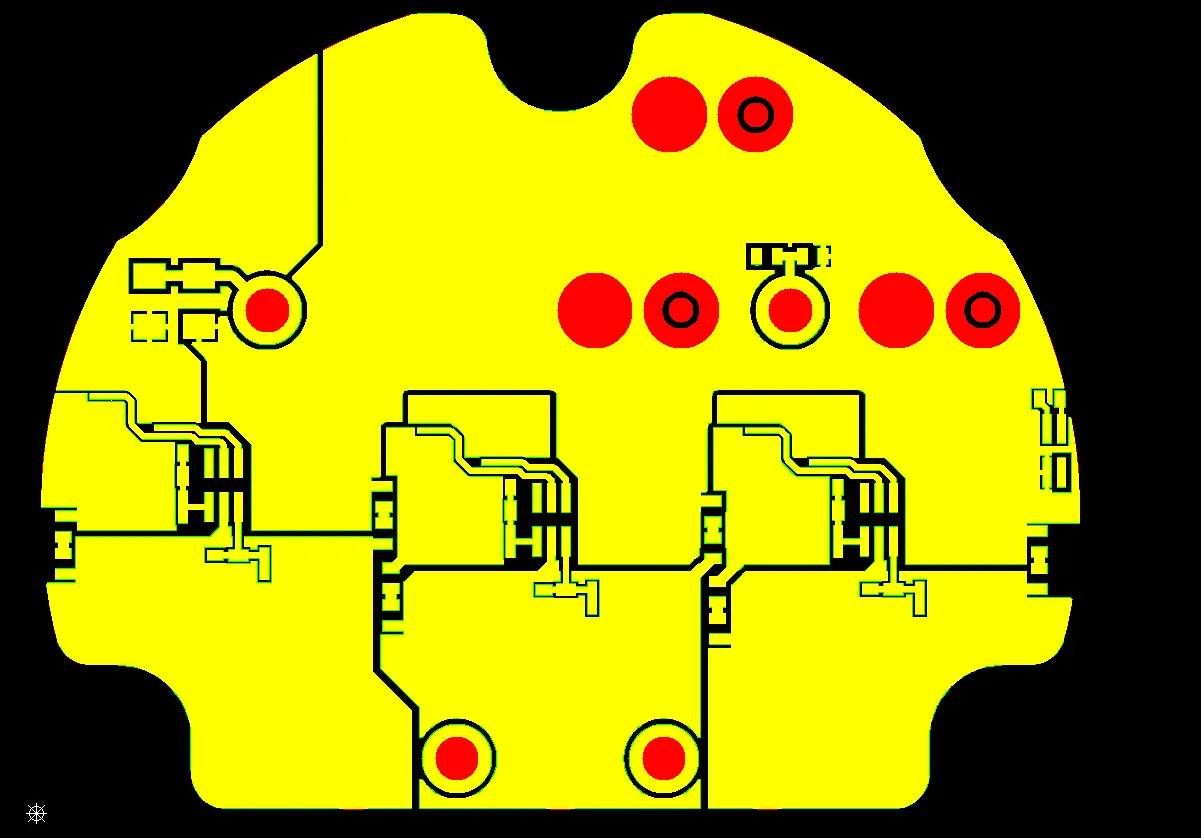
During CAM review of a heavy-copper multilayer FR-4 board, our engineering team identified several process constraints that required immediate clarification. From a DFM perspective, the primary concern was manufacturing stability under the more aggressive etching and plating conditions that heavy copper demands. Without confirmation, the design risked incomplete etching, residual copper bridges, unreliable via filling, and extended material lead times that could disrupt the production schedule. This case illustrates practical heavy copper PCB design rules focused on etch compensation, via plugging limits, and stackup flexibility.
The order ( #FR4-20260426-036 ) involved thick copper construction (commonly 3 oz or greater on outer or inner layers), resin-filled vias restricted to 0.3 mm diameter, a customer-specified stackup using special high-Tg or high-thermal material, and panelization without edge copper pour or standard reflective fiducials and tooling holes. These features are typical for high-current or thermal-management applications, yet they introduce tighter process windows that must be verified before etching and lamination begin.
Why Heavy Copper Construction Required Early Process Confirmation
Our CAM engineer first noted that the design carried heavy copper and lacked both reflective points and positioning holes on the process edge, while the board edge itself carried no copper pour. On heavy-copper panels these features are important for optical registration and mechanical handling during the longer etch cycles required for thicker copper. Simultaneously, the via-fill request was limited to 0.3 mm holes only, the stackup required a minor material substitution, and several pad-to-pad or pad-to-trace gaps were below the reliable clearance after etch compensation.
Further review revealed inconsistencies in the material call-outs between different sections of the documentation and a procurement note that the special laminate had a lead time exceeding one month. These observations formed a clear set of risk indicators: aggressive etching of thick copper, restricted via-plugging diameter, material availability constraints, and missing edge features that affect panel processing.
| Feature Observed | Condition in Files | Primary DFM Risk |
|---|---|---|
| Heavy copper etching | Insufficient spacing after etch factor | Residual copper bridges or shorts |
| Via resin fill | Only 0.3 mm vias requested | Incomplete fill or void risk on larger holes |
| Stackup material | Special laminate, long lead time | Schedule delay or substitution needed |
Table 1 records the key observations that triggered the Engineering Question. The engineering takeaway is that heavy copper amplifies every clearance and material decision; early confirmation prevents both process defects and schedule overruns.
Heavy Copper Clearance, Via Fill and Material Substitution Risks
The highest-priority risk was insufficient conductor spacing after accounting for the etch factor of thick copper. Heavy copper requires longer etch times and produces greater lateral undercut; gaps that appear adequate on the design screen can close or leave residual copper after processing. A second risk involved the restriction of resin plugging to 0.3 mm vias only. Larger holes left unfilled can trap chemistry or create voids that later cause reliability issues under thermal cycling. The third major risk was the special laminate whose procurement lead time exceeded one month, forcing a decision between schedule delay and a controlled stackup substitution.
Secondary observations included the absence of edge copper pour, reflective fiducials and tooling holes on the process border, and minor inconsistencies in the material documentation. These items affect panel handling and optical registration but were secondary to the etch, fill and material-availability issues.
From a DFM perspective the priority sequence was clear: compensate clearances by controlled pad shaving where necessary, confirm the 0.3 mm via-fill limit, and obtain agreement on either the original special material (with its long lead time) or an approved alternate stackup.
How Heavy Copper Process Limits Affect Yield and Reliability
If production had continued without addressing the tight clearances, the longer etch cycle required for thick copper would have left residual copper bridges or reduced the final spacing below safe electrical limits. According to common IPC-2221 spacing guidance and practical etch-factor experience, heavy copper PCB designs must incorporate additional compensation; otherwise short circuits or high-voltage failures appear after fabrication. On high-current boards these residual bridges also create localized hot spots that accelerate dielectric degradation.
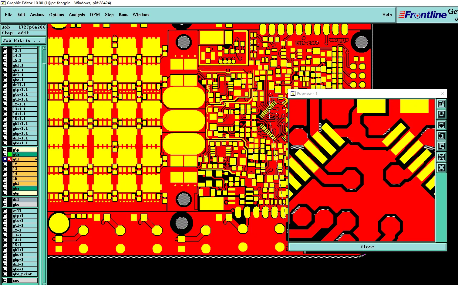
Figure 1: tight clearances
Restricting resin fill to only 0.3 mm vias leaves larger holes open. Unfilled vias can retain plating chemistry, create air voids, or allow solder wicking during assembly. Based on IPC-6012 and IPC-A-600 considerations, voids or incomplete fill in plated holes are process indicators that can compromise long-term via reliability, especially under thermal cycling typical of power applications.
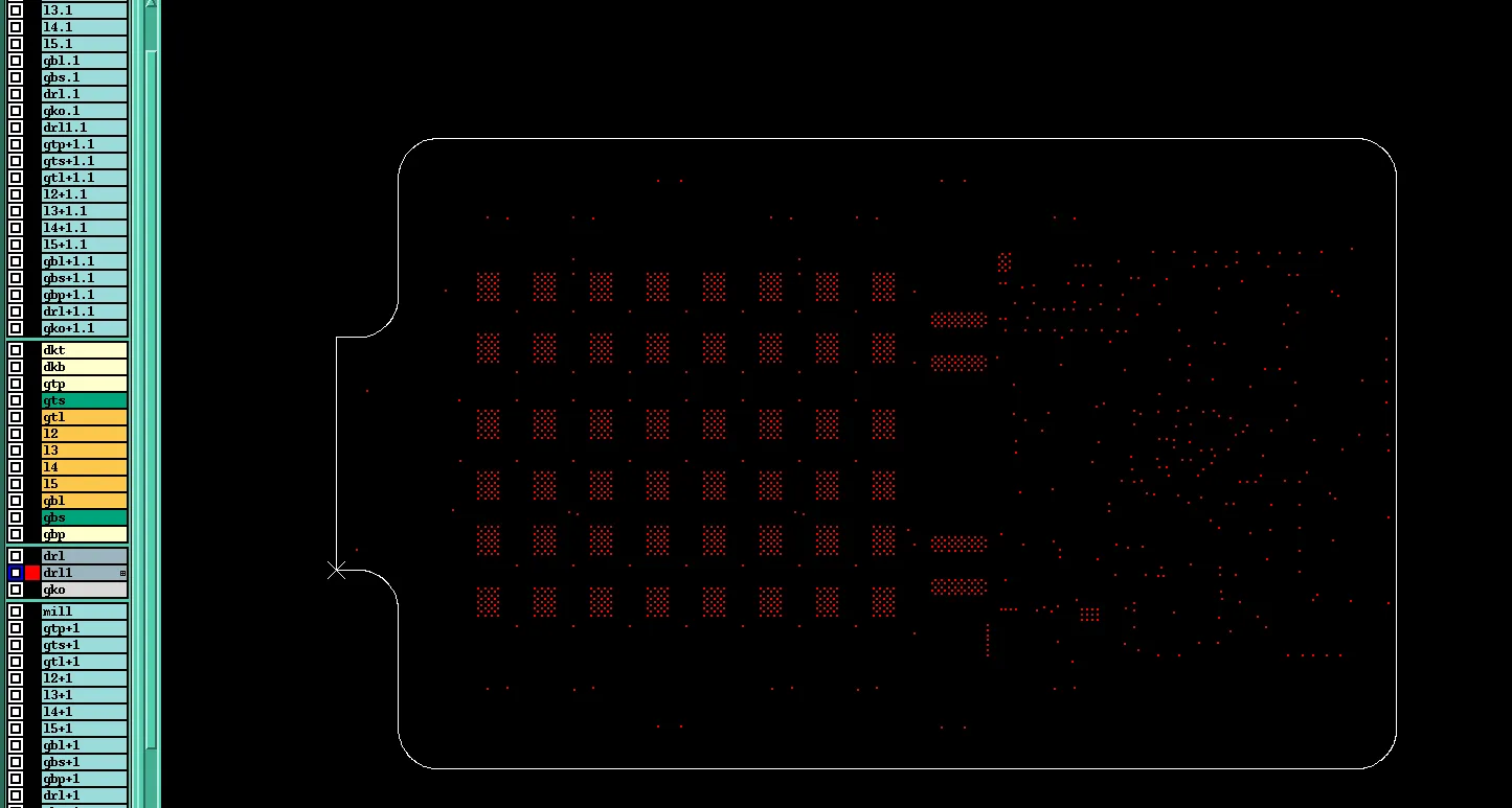
Figure 2: restricting resin fill to only 0.3 mm vias
Proceeding with the original special laminate without confirming the one-month-plus lead time would have delayed the entire order. A last-minute material change without customer agreement risks altering impedance, thermal performance or glass-transition temperature, potentially affecting both electrical and mechanical reliability.
| Potential Failure Mode | Root Cause Linked to EQ | Production or Field Impact |
|---|---|---|
| Residual copper bridges / shorts | Insufficient spacing after heavy-copper etch | Electrical failure, scrap after etch |
| Via voids or incomplete fill | Resin plug limited to 0.3 mm only | Reliability degradation under thermal stress |
| Schedule overrun | Special material lead time >1 month | Delayed shipment, potential redesign |
| Edge registration or handling issues | No edge copper, no fiducials or tooling holes | Process delays or panel damage |
Table 2 maps each realistic failure mode to the Engineering Question items. The engineering takeaway is that heavy copper multiplies the consequences of every clearance and material decision.
Failure Scenarios the Engineering Team Sought to Prevent
Had the original tight clearances remained uncompensated, the heavy-copper etch would have produced residual copper bridges. These bridges fail high-voltage or continuity testing and, if undetected, create hot spots that degrade the laminate over time. On a high-current design the thermal and electrical consequences are especially severe.
Leaving larger vias unfilled while only plugging 0.3 mm holes would have allowed chemistry entrapment or air voids. Subsequent thermal cycling can crack the via barrel or open the circuit, producing field failures that are difficult to diagnose. Proceeding with the long-lead special material without confirmation would have pushed the delivery date out by more than a month, forcing either a costly expedite or a last-minute stackup change that itself introduces new risk.
The absence of edge copper pour, reflective points and tooling holes further complicates panel handling on heavy-copper jobs, where the panels are heavier and more prone to registration drift during the extended process cycles. All of these scenarios share a common origin: insufficient design-for-manufacturing margin under the process conditions of thick copper.
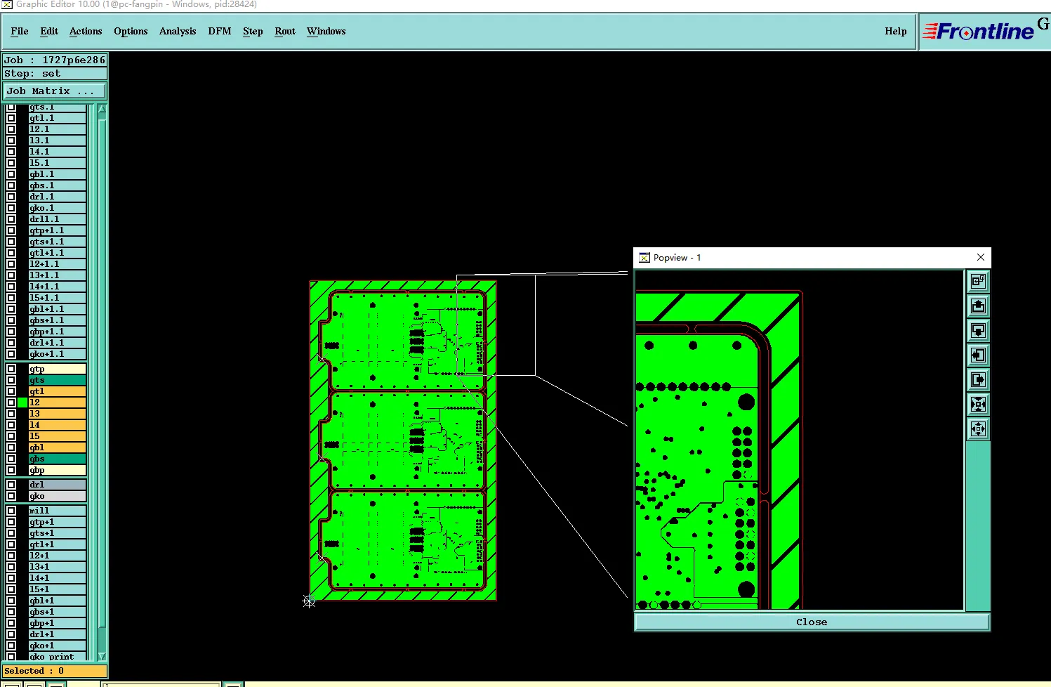
Figure 3: there are no fiducial marks or tooling holes on the process edge, and the edge rail has no copper pour
Preventive Actions Confirmed During the DFM Exchange
Our engineering team issued a focused Engineering Question that first addressed the insufficient spacing. Where gaps were too small after etch-factor compensation, controlled pad shaving was proposed to restore safe clearance while preserving electrical connectivity. The customer accepted this adjustment.
For the via-fill limitation the team confirmed that resin plugging would be applied only to 0.3 mm vias, matching the factory capability and avoiding incomplete fill on larger diameters. The stackup was reviewed in light of the special-material lead time exceeding one month; a minor, electrically equivalent substitution was proposed and accepted so that production could proceed on schedule. Material call-out inconsistencies between documentation sections were clarified and aligned. The absence of edge copper, reflective fiducials and tooling holes was noted and accepted after confirmation that the panel could still be processed reliably.
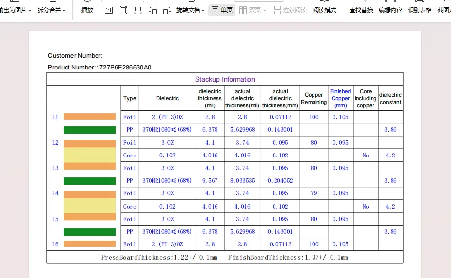
Figure 1: stack-up adjustment
With these decisions locked, the CAM data were updated: clearances were compensated by pad shaving where required, via-fill rules were set to the 0.3 mm limit, the approved alternate stackup was adopted, and the order was released. The revised design retained the intended high-current and thermal performance while eliminating the primary sources of etch defects, via voids and schedule risk.
| Action Item | Customer Decision | Manufacturing Benefit |
|---|---|---|
| Insufficient spacing | Pad shaving accepted | Safe clearance after heavy-copper etch |
| Via resin fill | Limited to 0.3 mm vias | Reliable fill, no voids on larger holes |
| Special material lead time | Stackup substitution approved | On-schedule production without performance loss |
Table 3 documents the closed decisions that converted a high-risk heavy-copper design into a manufacturable product. The engineering takeaway is that etch compensation, via-fill diameter limits and material flexibility form the core of practical heavy copper PCB design rules.
Building Trust Through Early Heavy-Copper Process Verification
This case demonstrates that heavy copper is not simply thicker copper; it changes etch behavior, via-filling capability and material lead-time dynamics. By identifying the clearance shortfalls, the 0.3 mm via-fill limit and the special-material procurement constraint during CAM review, the engineering team prevented residual copper bridges, via voids and multi-week schedule delays. Explicit customer agreement on pad shaving, fill rules and stackup substitution protected both first-pass yield and delivery commitment.
Designers working with heavy-copper boards are encouraged to incorporate etch-factor compensation in the original layout, specify via-fill diameters that match process capability, verify material availability early, and request DFM feedback on edge features and clearances. These practices convert potential manufacturing and schedule problems into controlled, documented decisions before production begins.
Proactive application of heavy copper PCB design rules remains one of the highest-leverage actions a DFM team can take when releasing high-current or thermal-management multilayer boards.
FAQ
Q1: Why does heavy copper require additional clearance compensation?
A1: Thicker copper needs longer etch times and produces greater lateral undercut. Gaps that look adequate on the design can close or leave residual bridges after etching, creating shorts or reduced electrical spacing.
Q2: Why limit resin plugging to 0.3 mm vias on some processes?
A2: Process capability for complete, void-free fill is often restricted to smaller diameters. Attempting to fill larger holes can leave chemistry traps or air voids that later cause via cracking under thermal cycling.
Q3: What happens if a special laminate has a long procurement lead time?
A3: The entire order is delayed unless an electrically and thermally equivalent alternate stackup is approved. Early confirmation allows the substitution to be made without last-minute risk to performance or schedule.
Q4: Why is pad shaving sometimes used on heavy-copper designs?
A4: Controlled reduction of pad size restores the minimum clearance after etch compensation while still providing adequate annular ring and solderable area. It is a practical DFM compromise when the original spacing is marginal.
Q5: How do missing edge copper and fiducials affect heavy-copper panels?
A5: Heavy-copper panels are heavier and undergo longer process cycles. Edge copper, reflective points and tooling holes improve registration accuracy and mechanical handling; their absence increases the chance of process variation or panel damage.
Q6: How can designers avoid similar issues on future heavy-copper boards?
A6: Incorporate etch-factor compensation in the original layout, specify via-fill diameters that match factory capability, verify special-material lead times early, provide adequate edge features, and request DFM review of clearances and stackup. These steps form the practical foundation of reliable heavy copper PCB design rules.