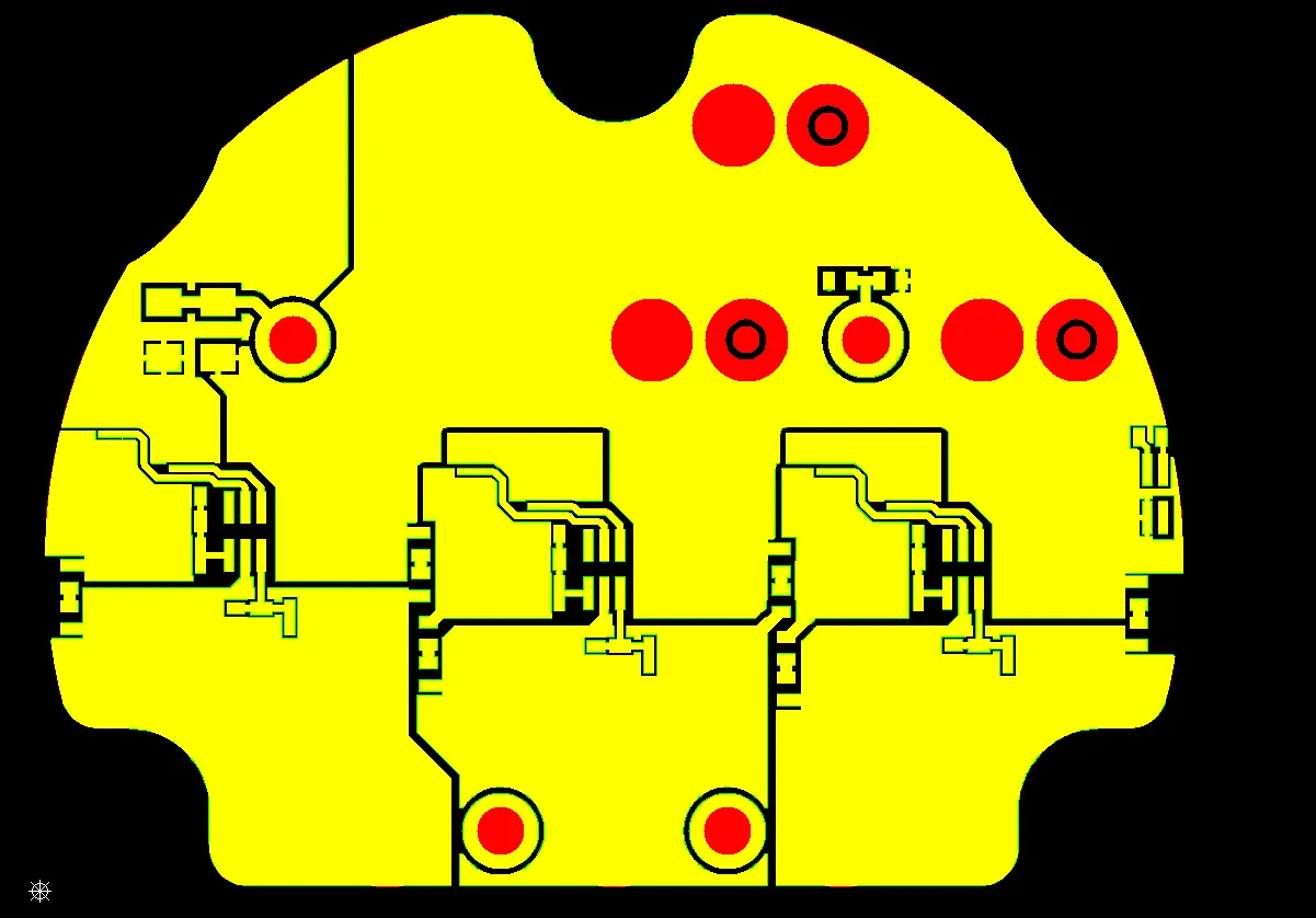
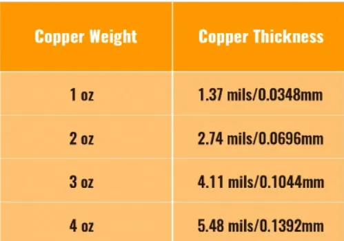
A 1-layer FR-4 board measuring 250 mm × 109 mm came in for CAM review. The order called for 2.0 mm thickness, TG150 material, 1 oz / 2 oz copper, green solder mask on both sides, white silkscreen, lead-free HASL, and via openings. Quantity was 200 single pieces. The customer had sent both Gerber and ODB++ files. At first glance the data looked usable, but the Gerber set showed top and bottom circuit layers, top and bottom solder-mask layers, and top and bottom silkscreen layers. Several of those layers were completely empty. The production drawing, however, clearly described a single-sided board. A slot also sat too close to the board edge, and a string of characters appeared on the drawing but not in the files. These mismatches left us unable to decide the correct layer count, plating path, or outline treatment. We had to settle the question before any tooling could start.
What the Designer Appeared to Want
The order ( #FR4-20260509-048 ) parameters and the production drawing both pointed to a simple 1-layer board. Copper was listed as 1 oz inner / 2 oz outer, yet on a true single-sided part the "inner" label usually does not apply. The Gerber package still carried a full dual-sided layer stack. Top circuit, top solder mask, and bottom silkscreen were blank. Bottom circuit and bottom solder mask carried the real features. The most likely explanation was that the designer had exported a double-sided template and simply left the unused side empty. Still, the files themselves did not say so. Without a clear statement we could not know whether to treat the board as single-sided or to process both sides.
Empty Layers That Looked Like Real Ones
We compared every layer against the production drawing. Only one circuit layer held copper. The opposite side was blank. Solder mask existed in the file header on both sides, but the top mask layer was empty while the bottom mask held the openings. Silkscreen followed the same pattern. Hole copper was listed as 0 µm, which fits a non-plated or single-sided construction, yet the dual-sided headers remained. If we had processed the empty layers as functional, the board would have received unnecessary plating or mask chemistry on a side the designer never intended to use. AOI set up for a double-sided part would also have flagged the blank side as missing features and generated false rejects.
The risk was straightforward. An incorrect assumption about layer count would change process flow, copper calculations, surface-finish cost, and final appearance. The finished boards would no longer match the single-sided drawing the customer had approved.
| Layer in Gerber | What We Found | Order / Drawing Intent | If We Misread It |
|---|---|---|---|
| Top Circuit | Empty | Not needed | Extra plating or etch |
| Bottom Circuit | Populated | Functional side | None if selected correctly |
| Top Solder Mask | Empty | Not needed | Unnecessary mask process |
| Bottom Solder Mask | Populated | Required | None if selected correctly |
| Bottom Silkscreen | Empty | Characters shown on drawing | Missing legend |
The Core Problem: Layer Count That Could Go Either Way
The real conflict sat between the file structure and the order. The Gerber and ODB packages still carried dual-sided layer names even though several layers were blank and the production drawing called for a 1-layer board. In CAM practice an empty layer is not automatically ignored. The system needs a clear instruction on which layers are real. Without that instruction we could not set the plating sequence, mask application, or inspection criteria with any confidence.

Figure 1: Gerber and ODB packages
Two readings were possible. The designer may have started from a double-sided template and simply left one side unused. Or the board might actually need features on both sides and the drawing was incomplete. Those two readings lead to different process flows, different copper weights, and different costs. We could not choose one without customer confirmation.
Slot Clearance and Missing Characters
Other details added weight to the need for clarification. One slot sat close enough to the outline that routing would leave little residual material. On a 2.0 mm board that raises the chance of breakout, sharp corners, or burrs that fail normal edge-quality checks. The production drawing also showed a string of characters that did not appear in any silkscreen layer. Board dimensions stated by the customer did not match the measured Gerber outline, and the 2.0 mm thickness came without a tolerance. Each of these points needed its own answer, yet all of them depended on the layer-count decision. Once we knew the board was truly single-sided, we could identify the correct copper side, mask side, and legend side and then settle the edge and dimension questions against that baseline. To see how factory CAM teams systematically catch these discrepancies, read our guide on
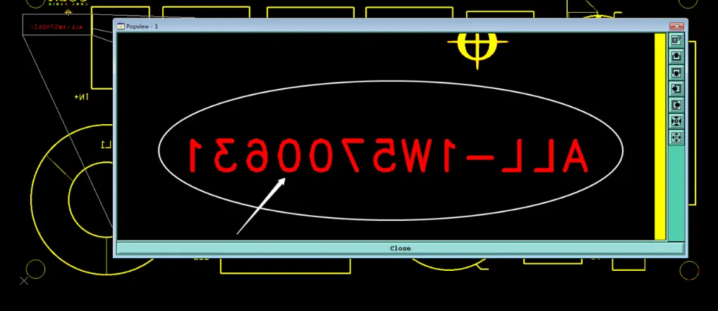
Figure 2: a string of characters that did not appear in any silkscreen layer
How We Locked the Board as Single-Sided
We told the customer we would treat the Gerber set as the manufacturing source and ignore the empty top circuit, top solder-mask, and bottom silkscreen layers. The board would be built strictly as 1-layer single-sided PCB. The character string on the drawing would be added only if the customer confirmed it was required. For the slot we offered either a small outline adjustment or acceptance of the existing clearance with the understanding that minor breakout risk remained. Dimension and thickness questions were sent back for a single authoritative answer.
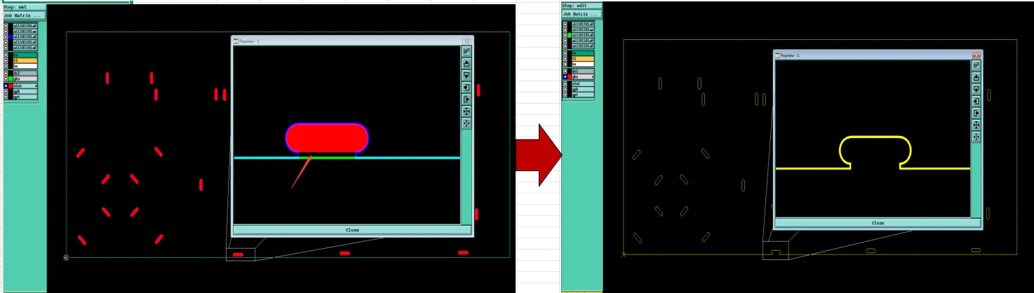
Figure 3: the slot sat too close to the outline
The customer agreed. The empty layers were stripped, the outline and slot were adjusted as directed, and thickness was locked at 2.0 mm with the stated tolerance. Once the layer-count question was settled, the secondary issues closed quickly. The 200-piece order moved forward as a true 1-layer board.
| What We Saw | Conflict | What We Proposed | Final Result |
|---|---|---|---|
| Empty dual-sided layers in Gerber | Layer count vs 1-layer order | Ignore empty layers; build single-sided | Confirmed |
| Slot too close to edge | Breakout and burr risk | Adjust outline or accept residual risk | Adjusted |
| Characters on drawing missing from Gerber | Incomplete legend | Add only if required | Resolved |
| Dimension and thickness mismatch | No single authoritative value | Use customer-confirmed numbers | Locked |
Practical Takeaways for Cleaner Single-Sided Files
- If the board is truly single-sided, remove the unused circuit, mask, and silkscreen layers from the Gerber or ODB output. Empty layers invite misinterpretation.
- Leaving blank layers in a dual-sided template creates plating, mask, and inspection questions even when the drawing is clear.
- Slots and holes need enough edge clearance on the finished outline. Features that risk breakout or burrs will always draw an Engineering Question on mechanically formed boards.
- Any text that appears on the production drawing but is missing from the Gerber silkscreen must be confirmed or added before release.
- Board thickness and overall dimensions in the order must match the measured Gerber data. Discrepancies need one clear source before tooling starts.
- A hole-copper value of 0 µm fits non-plated or single-sided construction. Pair it with clear plating attributes so the intent is unambiguous.
- When both Gerber and ODB files are supplied, make sure both sets describe the same layer content and the same single-sided or double-sided intent.
FAQ
Q1: Why do empty dual-sided layers in a Gerber set cause an Engineering Question on a 1-layer order?
A1: CAM systems read the layer headers. Empty layers are not automatically discarded. Without a clear instruction the factory cannot know whether the board is truly single-sided or whether the blank side was meant to carry features.
Q2: What goes wrong if empty layers are processed as real?
A2: The board may receive plating or mask chemistry on a side the designer never intended. Copper weights can be calculated incorrectly, and AOI set up for a double-sided part will flag the blank side as missing features.
Q3: Why is a slot too close to the board edge a problem on 2.0 mm material?
A3: Routing leaves too little residual material. The result can be breakout, sharp corners, or burrs that fail normal edge-quality checks and create handling issues.
Q4: What should a designer do when characters appear on the production drawing but not in the Gerber silkscreen?
A4: Add the characters to the silkscreen layer before release, or state clearly that the drawing text is for reference only and must not be fabricated.
Q5: Why does board thickness need a tolerance even when the nominal value is 2.0 mm?
A5: Commercial laminate varies within normal tolerances. Without a stated allowance the factory cannot decide whether a measured deviation is acceptable or requires rejection.
Q6: When both Gerber and ODB files are supplied, which set should control production?
A6: The factory selects one authoritative set after confirming that both describe the same layer content and the same single-sided or double-sided intent. Contradictory sets always require clarification.
```