 00:54
00:54
Single-Sided PCB
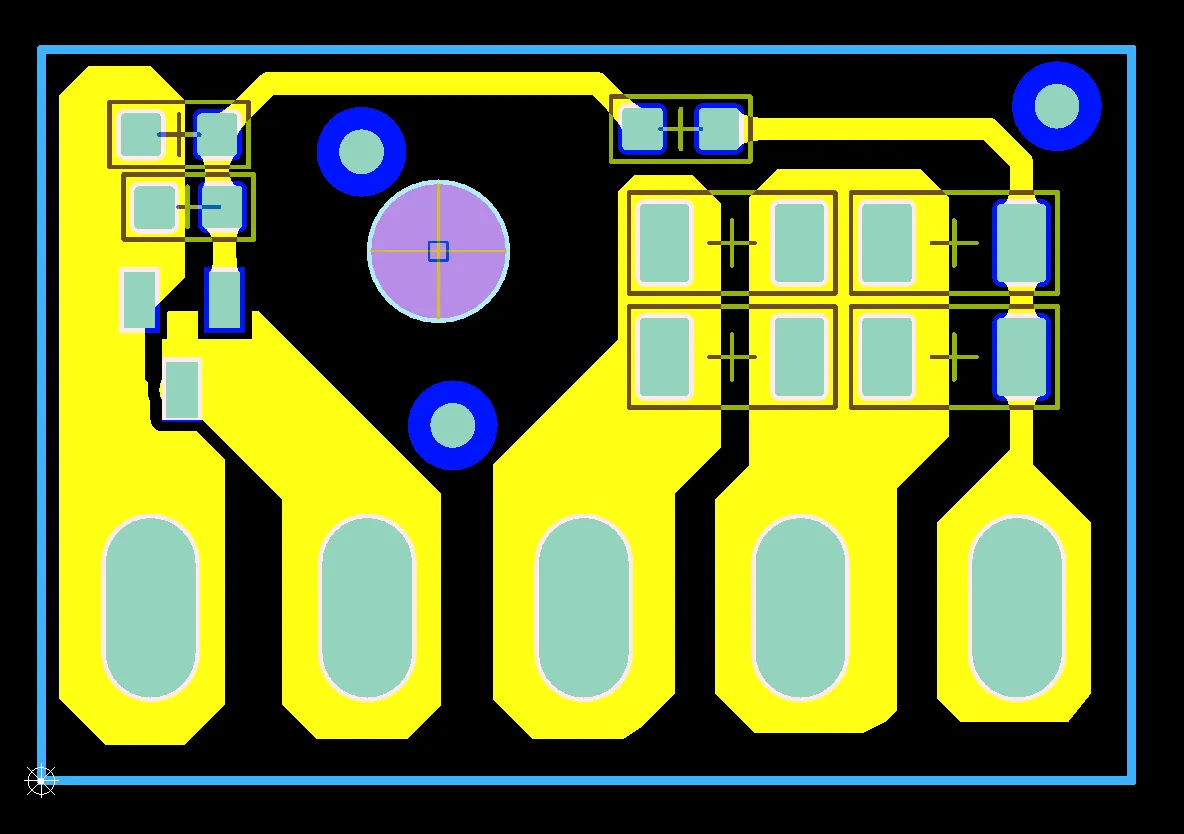
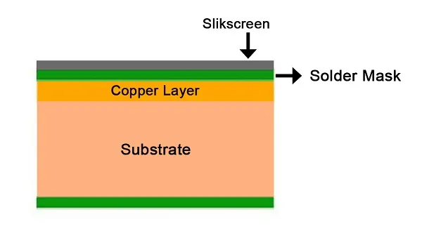
Single-sided PCBs represent a fundamental building block in electronics design, featuring conductive traces, pads, and components mounted on just one side of the board. This configuration simplifies manufacturing and reduces costs, making it an ideal choice for beginners, hobbyists, and applications where complexity is minimal. Professionals often turn to single-sided PCBs for prototypes, low-density circuits, or devices like basic sensors, LED displays, and simple control systems. By limiting traces to one layer, these boards avoid the need for vias or multilayer routing, which streamlines the etching process and minimizes errors during assembly. Understanding the advantages of single-sided PCBs can guide effective project decisions. They offer quicker turnaround times in production and are easier to troubleshoot, as all connections are visible on a single surface. For instance, in educational settings or DIY projects, users appreciate the straightforward layout that allows for manual soldering without advanced tools. However, to maximize reliability, best practices include optimizing trace widths to handle current loads, ensuring adequate spacing to prevent shorts, and incorporating ground planes where possible to reduce noise. Common applications span consumer electronics, automotive modules, and medical devices, where cost efficiency outweighs the need for high-density interconnects. For those delving deeper into single-sided PCB design, considerations such as material selection—typically FR-4 for its durability—and software tools like Eagle or KiCad can enhance outcomes. Articles under this tag provide detailed guides on layout techniques, fabrication methods, and comparisons with double-sided alternatives, helping users refine their skills and avoid pitfalls like overheating or signal interference. Whether you are prototyping a new gadget or scaling a simple circuit, the resources here offer practical strategies to achieve robust, efficient results.
Video Guide
-
00:54
Technical Articles
DIY PCB Fabrication: Essential Tools and Techniques for the Home Lab
Common 1 Layer FR4 PCB EQ Issues: How Manufacturers Review Gerber Files
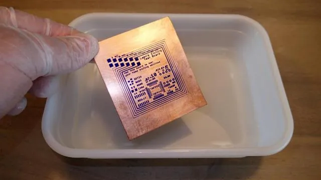
Single Sided PCB Etching: Choosing the Right Chemicals
Optimizing Single Sided PCB Layout for Minimal Noise
Mastering CEM 1 PCB Design: A Comprehensive Guide for Beginners
CEM 1 PCB: The Budget Friendly Choice for Single Layer Electronics?
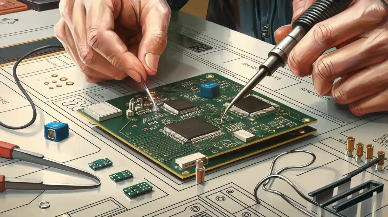
Single Sided PCB Assembly: A Step by Step Guide
Designing for Manufacturability: Single Sided PCB Best Practices
PCB Manufacturing Process for Beginners: From Schematic to Finished Board

Single-Layer Aluminum PCB Engineering Case: Machining Limits, Edge Clearance & Material Thickness Challenges
Optimize Your CEM 1 PCB Design: Mastering Trace Width and Spacing
CEM 1 for Audio Amplifiers: A Cost Effective Solution for Clear Sound
Building a Simple Radio Receiver with a Single-Layer PCB
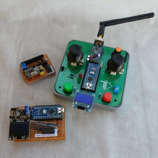
Single-Sided PCB: The Backbone of Simple Remote Controls
Mastering the FR-1 PCB Manufacturing Process: A Step-by-Step Guide
Get in Touch
Send Message
- Products & Service
- Company
- About AIVON
- Contact
- News
- Blog
- Certification
-


- Payment
-


2026 AIVON.COM All Rights Reserved