










A recent single-layer aluminum base PCB order for thermal management applications featured a compact 11.3 x 7 mm footprint, 1.0 mm thickness, 1 oz copper, white solder mask on top, and lead-free HASL finish. With 150 pieces required in 5-set panels, manufacturing precision was essential to maintain thermal performance and mechanical integrity.
From a DFM perspective, aluminum PCBs introduce unique challenges compared to standard FR-4, particularly around countersink holes near edges, panelization with V-cut and routing, tight copper clearances, and silkscreen placement. Our engineering review identified risks that could have led to edge defects, burrs, and reliability concerns if left unaddressed.
Project Context and Need for Thorough DFM Review
This aluminum substrate board ( #ALU-20260121-011 ) was designed for heat dissipation in electronics, leveraging 8.0W/m·K thermal conductivity. The single-layer construction with mechanical forming and mixed depanelization (V-cut plus routing) created several manufacturability considerations. Small board size combined with countersink holes and tight tolerances to the outline amplified potential issues during drilling, routing, and panel separation.
DFM review was critical because aluminum base materials behave differently under mechanical stress and thermal processing than standard laminates. Without clarification, minor design features could result in yield loss or compromised thermal paths in the final product.
Key Manufacturability Challenges in Aluminum Base Design
The primary risks centered on countersink hole proximity to the board edge, panelization spacing for V-cut and routing, and copper clearance adjustments near the outline. These issues are particularly significant on aluminum PCBs due to material hardness and the need to preserve edge quality for thermal contact and mechanical stability.
Additional points included silkscreen adjustments to avoid printing on pads and confirmation of non-plated hole processing on a single-layer aluminum design. The proposed panel layout of 6x5 with 5 mm process edges on all sides required careful validation to minimize burrs and residue after depanelization.
| Risk Area | Design Feature | Manufacturing Concern |
|---|---|---|
| Countersink Holes | Proximity to board edge | Edge breakout and mechanical weakness |
| Panelization | V-cut + routing with tight gaps | Burrs, residue, and panel damage |
| Copper Clearance | Trace to outline spacing | Shorts or exposed copper after processing |
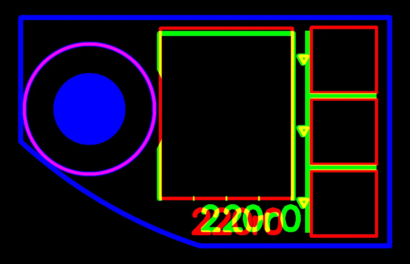
Figure 1: silkscreen adjustments to avoid printing on pads
How Identified Risks Impact Yield and Long-Term Reliability
Countersink holes positioned too close to the edge could lead to breakout during drilling or forming, weakening the board perimeter and affecting thermal interface contact. On aluminum substrates, such defects can propagate under mechanical or thermal cycling, potentially causing delamination or reduced heat dissipation efficiency.
Inadequate panelization spacing risked excessive burrs and residual material after V-cut and routing separation. This not only impacts cosmetic acceptance but can introduce conductive debris that causes shorts during assembly or in-field operation. According to IPC-A-600 considerations, edge quality directly influences acceptability for boards requiring reliable mechanical and thermal performance.
Tight trace-to-outline clearances necessitated copper reduction. Without controlled adjustment, this could result in shorts, exposed copper, or inconsistent etching on the aluminum base, compromising both electrical isolation and long-term corrosion resistance.

Figure 2: the trace spacing and the distance to the board outline are too close
| Risk Factor | Potential Yield Impact | Reliability Consequence |
|---|---|---|
| Edge Breakout | Increased scrap rate | Thermal interface failure |
| Burrs from Depanel | Post-process cleaning issues | Assembly shorts or contamination |
Failure Scenarios the DFM Team Aimed to Avoid
If the countersink hole proximity had been ignored, drilling from the circuit side could have caused severe edge breakout, leading to scrap boards or mechanically compromised units. In application, this might result in poor thermal contact, overheating, or physical failure under vibration — common concerns for aluminum base designs in power or LED applications.

Figure 3: countersunk holes are too close to the board edge
Zero-spacing panelization as originally indicated would likely produce excessive burrs and material residue after routing. Such defects often require additional manual deburring, increasing costs and risking incomplete removal that leads to assembly failures or cosmetic rejects. Our experience shows these issues frequently escalate on aluminum materials due to their hardness.
Uncontrolled copper reduction near the outline risked shorts or exposed base material, potentially causing electrical failures or accelerated corrosion in humid environments. Silkscreen placement adjustments were also critical to prevent ink on pads, which could impair solderability and lead to weak joints.
Recommended Preventive Actions and Client Collaboration
We recommended accepting controlled edge breakout on specific countersink holes while confirming drilling direction and parameters to minimize impact. For panelization, we proposed and confirmed a revised 6x5 layout with 2.0 mm X-axis and 5.0 mm Y-axis spacing plus 5 mm process edges on all sides to effectively reduce burrs and residue.
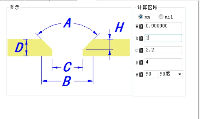
Figure 4: manufacture the countersunk holes on the PCB according to the dimensions shown in the image
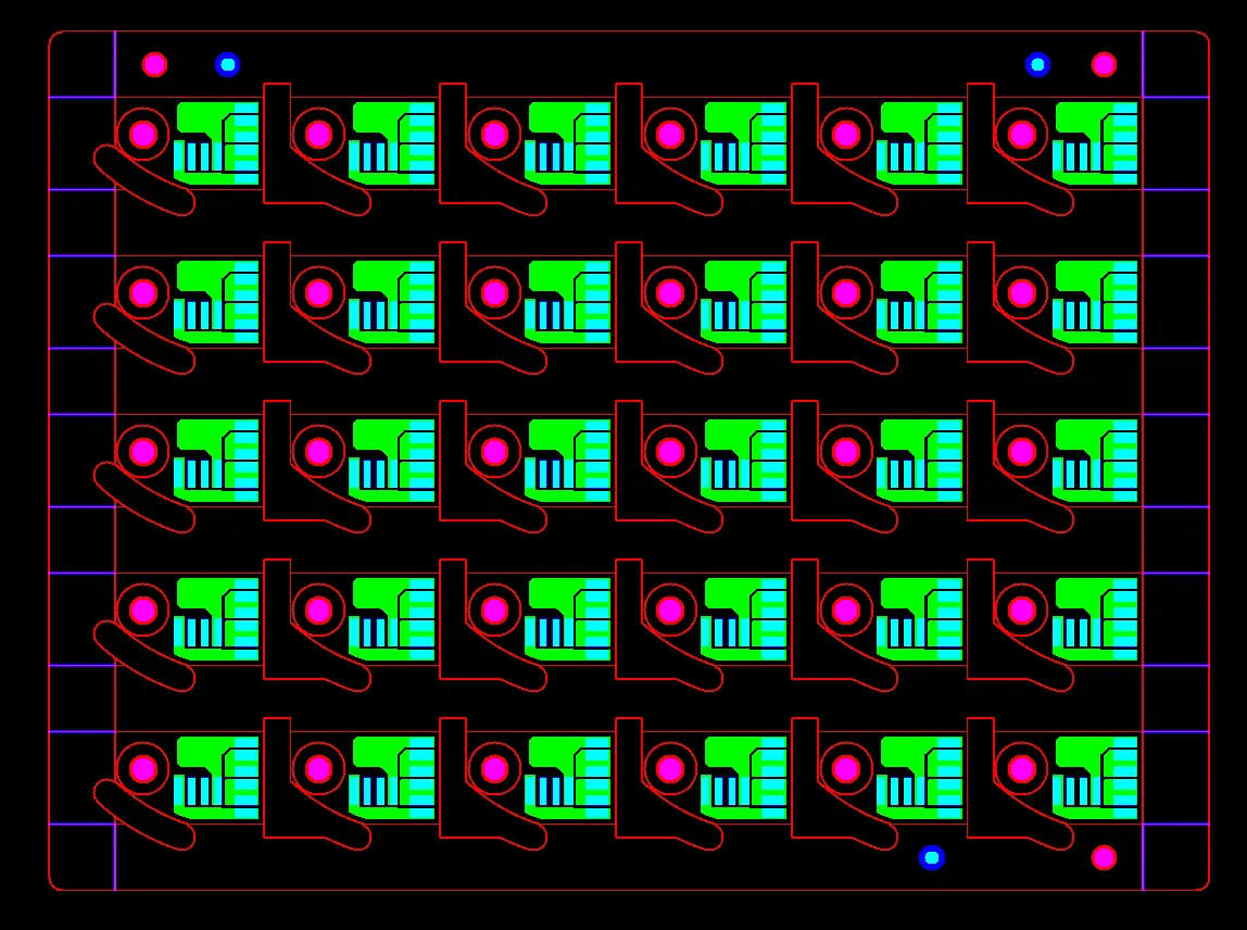
Figure 5: 6x5 layout with 2.0 mm X-axis and 5.0 mm Y-axis spacing plus 5 mm process edges
Copper reduction was applied strategically in tight areas to maintain isolation without over-etching. Silkscreen characters and frames were adjusted with enlargement and movement, accepting minor incompleteness where necessary to avoid pad interference. Non-plated hole processing was confirmed as standard for this single-layer aluminum design.
Production numbering was added to the process edge due to insufficient internal space. All changes were documented with gerber references and shared for client approval, allowing quick confirmation and smooth transition to production.
| Action Taken | Rationale | Outcome |
|---|---|---|
| Revised Panel Layout | Optimized spacing for V-cut/routing | Reduced burrs and improved edge quality |
| Countersink Confirmation | Acceptable breakout limits | Maintained structural integrity |
| Copper & Silkscreen Adjustments | Avoid shorts and pad contamination | Enhanced solderability and yield |
The collaborative process demonstrated how targeted engineering questions resolve ambiguities efficiently, keeping the 12-day delivery on track while protecting product quality.
Strengthening Reliability Through Early DFM Engagement
This aluminum PCB case underscores the importance of addressing panelization, edge features, and clearance issues before fabrication. By resolving these risks proactively, we helped ensure clean edges, reliable thermal performance, and high yield on a 150-piece order.
Early DFM involvement allows designers to make informed decisions that balance functionality with manufacturability. We recommend submitting designs for review as soon as possible, especially for aluminum base boards with mechanical features or tight tolerances, to prevent issues that are far more costly to correct later.
FAQ
Q1: Why do countersink holes near the board edge require special DFM attention on aluminum PCBs?
A1: Proximity increases breakout risk during drilling and forming due to material properties. Unaddressed, this can weaken edges, affect thermal contact, and lead to field failures. Confirmation of acceptable limits prevents scrap and maintains structural reliability.
Q2: What problems can arise from insufficient spacing in PCB panelization with V-cut and routing?
A2: Tight or zero gaps often cause burrs, material residue, and rough edges after depanelization. On aluminum boards, this complicates cleaning and raises short circuit risks. Optimized spacing reduces post-processing effort and improves overall edge quality.
Q3: How does copper reduction help when traces are close to the board outline?
A3: Strategic copper pullback prevents shorts and exposed copper after etching. Without it, tight clearances risk electrical failures or corrosion. This adjustment is a standard DFM practice to ensure reliable isolation on finished boards.
Q4: Why adjust silkscreen placement on pads for single-layer designs?
A4: Ink on pads can severely impair solderability and joint strength. Enlarging or moving legends, even if it results in minor frame incompleteness, protects assembly quality and reduces defect rates.
Q5: What makes aluminum PCBs particularly sensitive to panelization and edge design choices?
A5: The harder base material and thermal requirements make edge quality and burr control more critical. Poor choices can affect both mechanical durability and heat transfer performance. DFM review ensures the design aligns with practical fabrication constraints.






