Introduction
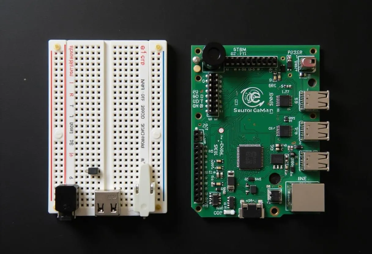
Breadboards offer a fast way for electronic hobbyists to test circuits without soldering. They allow quick changes and rearrangements, making them ideal for initial prototyping. However, as projects grow in complexity, breadboards reveal limitations like loose connections, size constraints, and unreliable performance under vibration or power. Transitioning to a printed circuit board (PCB) makes your design permanent, compact, and robust for real-world use. This guide covers how to transfer breadboard circuit to PCB, including PCB design from schematic and easy PCB fabrication for hobbyists. You'll learn practical steps for making a PCB at home using methods like the toner transfer PCB method and DIY PCB etching.
Breadboard vs PCB: Why Make the Switch?
Breadboards excel in temporary setups but falter in permanent applications due to their mechanical nature. Wires can shift, causing intermittent failures, and the setup occupies more space than a custom board. PCBs provide soldered connections that withstand environmental stresses, reducing failure rates in ongoing projects. For hobbyists building devices like sensors or amplifiers, a PCB ensures consistency and professionalism. This shift also prepares designs for scaling, whether for personal use or sharing with communities. Ultimately, making your projects permanent unlocks reliability that breadboards simply cannot match.
PCBs follow established design principles to achieve high performance. Standards like IPC-2221B guide layout to prevent issues such as signal interference or thermal problems. Hobbyists benefit by adopting these basics early, avoiding costly redesigns later.
Understanding PCB Design from Schematic
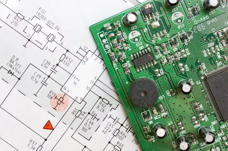
Start with your breadboard circuit's schematic, a diagram showing components and connections. To transfer breadboard circuit to PCB, convert this into a physical layout using PCB design software. Identify components, note their footprints, and map connections accurately. Group parts logically by function, like power sections near regulators, to minimize trace lengths. Consider layers: single-sided for simple hobby projects, double-sided for more complexity. Always verify netlist integrity to match the schematic exactly.
Layer stackup affects performance, even in home fabrication. For hobbyists, a 1.6 mm thick FR-4 substrate works well for rigidity. Route traces with widths suited to current: 0.5 mm for signals, wider for power. Add vias for double-sided boards to connect layers cleanly. Simulate if possible to check for shorts or opens before printing.
From Breadboard to PCB Layout: Step-by-Step Transfer
Document your breadboard setup first by photographing it and listing components. Draw or import the schematic, then place footprints on the PCB canvas. Position parts to mimic the breadboard flow, optimizing for shortest paths. Route traces avoiding sharp angles, which can cause etching defects. Generate Gerber files for fabrication, but for home use, prepare a mirror image for toner transfer.
Test the design virtually by running a design rule check. Ensure clearances meet minimums, like 0.2 mm between traces for hobby etchers. Label pads clearly for easy soldering later.
Toner Transfer PCB Method: Easy Home Fabrication
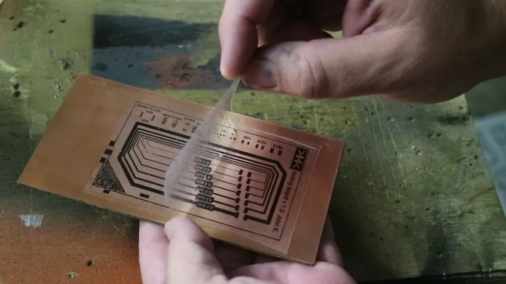
The toner transfer PCB method suits hobbyists for its simplicity and low cost. Print your mirrored PCB layout on glossy or toner transfer paper using a laser printer. The toner acts as an etch resist when transferred to copper-clad board. Clean the board with fine steel wool and isopropyl alcohol for perfect adhesion. Iron the printout onto the board at medium heat for 5-10 minutes, applying even pressure.
Peel off the paper once cooled, revealing toner traces. Touch up any breaks with a permanent marker. This method allows precise DIY PCB etching without special equipment.
DIY PCB Etching Process
Prepare etcher solution like ferric chloride or a safer cupric chloride mix, always in a well-ventilated area. Submerge the board toner-side up, agitating gently to expose copper evenly. Etching takes 10-30 minutes depending on temperature and concentration; warmer solutions speed it up. Rinse thoroughly with water, then neutralize with baking soda solution. Remove toner with acetone or lacquer thinner, leaving clean traces.
Safety is paramount: wear gloves, goggles, and avoid skin contact with chemicals. Dispose of waste per local regulations to protect the environment.
Post-etch, drill holes for through-hole components using a precision drill press. Inspect for defects like under-etching, which widens traces undesirably.
Best Practices for Easy PCB Fabrication for Hobbyists
Follow IPC-A-600 guidelines for visual acceptability, checking for clean edges and no bridges. Use 35 micron copper for standard hobby boards, balancing cost and etchability. For double-sided, align layers carefully before etching the second side. Bake boards at low heat post-etch to harden traces if needed.
Incorporate fiducials or alignment marks for precision. Test continuity with a multimeter before populating. Solder components starting with low-profile ones to avoid bridging. Learn more in our SMT assembly guide.
Common Troubleshooting in Home PCB Making
Blurry toner transfer often stems from poor paper or insufficient heat; try multiple passes. Pinholes in etching indicate weak resist; strengthen with additional marker strokes. Warped boards result from uneven heating; clamp during ironing. If traces lift during soldering, use flux and lower temperature.
Over-etched areas narrow traces, risking high resistance; enlarge in design next time. For persistent issues, review layout against IPC-6012E specs for qualification basics.
Advanced Tips for Hobbyist PCBs
Explore panelization for multiple boards per sheet to save material. Add silkscreen via another toner layer for labels. For SMD components, practice on scrap first using DIY SMT stencils. These elevate home projects to professional levels.
Conclusion
Moving from breadboard to PCB transforms prototypes into enduring electronics. By mastering PCB design from schematic and techniques like toner transfer PCB method, hobbyists achieve reliable results at home. Adhere to best practices and standards for quality outcomes. Experiment safely, iterate designs, and enjoy the satisfaction of custom boards. Your projects now stand ready for any challenge.
FAQs
Q1: How do I transfer breadboard circuit to PCB effectively?
A1: Start by creating a schematic from your breadboard setup, then use PCB software to place components and route traces. Verify connections match exactly via netlist comparison. Print mirrored layout for toner transfer, etch, and drill. Test bare board continuity before soldering. This ensures accuracy for easy PCB fabrication for hobbyists.
Q2: What is the toner transfer PCB method for making a PCB at home?
A2: Print layout on glossy paper with laser printer, transfer toner to copper board using iron. Etch away excess copper with ferric chloride solution. Clean and drill holes afterward. It's ideal for single or double-sided boards. Follow safety protocols for chemicals.
Q3: What are common pitfalls in DIY PCB etching?
A3: Uneven etching from poor agitation leads to incomplete removal. Weak toner resist causes pinholes; reinforce with marker. Overheating warps boards, so use steady iron temperature. Always rinse and neutralize etchant. Check against IPC standards for quality.
Q4: Can beginners handle PCB design from schematic?
A4: Yes, begin with simple circuits, focusing on component placement and trace routing. Use design rule checks for clearances. Practice with single-sided layouts first. Resources like standard guidelines help avoid errors. Progress to complex designs gradually.
References
IPC-2221B — Generic Standard on Printed Board Design. IPC, 2012
IPC-A-600K — Acceptability of Printed Boards. IPC, 2021
IPC-6012E — Qualification and Performance Specification for Rigid Printed Boards. IPC, 2015


