










In a recent 4-layer rigid-flex PCB order measuring 119.87 × 109.66 mm, the fabrication files and process notes presented a classic capability evaluation challenge centered on rigid-flex PCB stackup design. The board combined a 1.0 mm overall thickness rigid section with 0.2 mm flexible tails, PI stiffeners limited to two specific flex regions, and a customer note emphasizing stiffener dimensions of 5.5 mm width by 4.425 mm height. Surface finish was specified as ENIG, copper weights differed between regions, and the construction was declared asymmetrical with the flex layers placed on the outer side.
The critical manufacturing questions were not abstract design theory. They concerned whether an asymmetrical rigid-flex stackup could be laminated, plated, and finished within a ±0.1 mm total thickness tolerance while keeping warpage acceptably controlled, and whether the proposed PI stiffener arrangement at the gold-finger zones would survive repeated ZIF insertion without fracture. These issues triggered a formal engineering capability assessment before any production release.
Project Requirements and the Core Stackup Challenge
Customer documentation listed a 4-layer rigid-flex PCB ( #RFP-20260429-041 ) construction, 1.0 mm finished thickness, 1 oz outer copper on the rigid section, and a flex section using Shengyi SF305C material at 0.2 mm with 1/3 oz internal and 1 oz external copper. The rigid dielectric was specified as FR-4 Tg 155. Flexible tails carried PI stiffeners of 0.1 mm thickness only on two locations. Finger-zone finished thickness was defined as 0.3 ± 0.05 mm. Delivery quantity was five pieces, full electrical test, and the board was accepted for external manufacturing.
During CAM intake the first observation was immediate: the supplied Gerber data contained only three copper layers. Layer G1 appeared empty and G2 data was incomplete. The stated 4-layer build could not be reconciled with the artwork. In parallel, the stackup was confirmed as asymmetrical—the flex region sat entirely on one outer side of the rigid core. No process edge or panelization instructions were present. The customer note explicitly warned that stiffeners existed only on the two flex tails of the stated dimensions.
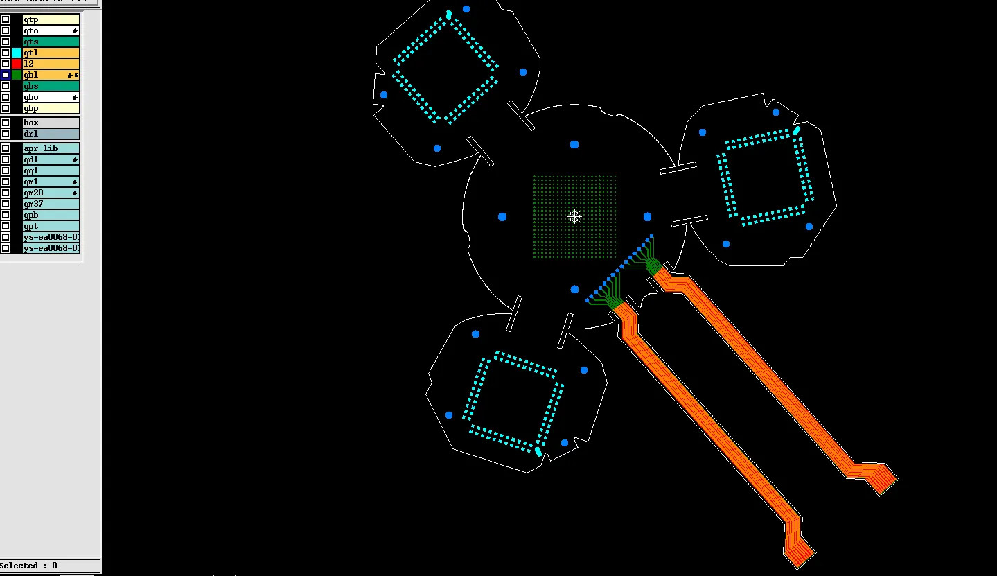
Figure 1: there are only three copper layers inside the gerber file
These observations raised three linked process-capability questions. First, could the missing copper-layer data be clarified so that a true 4-layer rigid-flex PCB stackup design could be built? Second, would the inherent asymmetry produce warpage beyond the 2 % acceptance limit already proposed by engineering? Third, would the PI stiffener geometry at the finger areas provide sufficient mechanical support for ZIF connector engagement without exceeding the fracture risk of the thin flex copper and coverlay stack?
| Parameter | Customer Request | Typical Process Window | Capability Assessment |
|---|---|---|---|
| Overall Thickness | 1.0 ± 0.1 mm | ±0.10–0.13 mm for hybrid builds | Achievable with tight lamination control |
| Flex Thickness | 0.2 ± 0.05 mm | ±0.03–0.05 mm on SF305C | Within capability |
| Finger Zone Thickness | 0.3 ± 0.05 mm | Dependent on stiffener + coverlay stack | Requires exact PI size match |
| Warpage | Accept 2 % | ≤1.5 % preferred for asymmetrical builds | Borderline; process controls mandatory |
Physical Limits of Asymmetrical Rigid-Flex Construction
An asymmetrical rigid-flex stackup places the flexible dielectric and copper exclusively on one face of the rigid core. During lamination the coefficient of thermal expansion mismatch between the FR-4 Tg 155 rigid section and the polyimide flex section generates residual stress. When the panel cools, the side carrying the flex tends to contract differently from the opposite rigid face, producing a predictable bow. Industry experience shows that pure asymmetrical constructions routinely exceed 1.5–2 % warpage unless countermeasures are applied.
IPC-6013 provides acceptance criteria for rigid-flex assemblies and notes that warpage and twist must be controlled relative to the finished outline. For boards of this size, a 2 % limit corresponds to roughly 2.2–2.4 mm maximum deviation across the long axis. That value is manufacturable, but only inside a narrow process window: balanced copper distribution, controlled cooling rate after lamination, and uniform pressure distribution across the hybrid panel.
Copper weight management added another constraint. The flex region used 1/3 oz internal and 1 oz external copper while the rigid section was 1 oz / 1 oz. Differential etch rates and plating thickness between the two zones can create local thickness steps at the rigid-to-flex transition. Those steps become stress concentrators if the coverlay or stiffener edges are not precisely registered. In practice, the transition zone requires a minimum 0.5–1.0 mm coverlay overlap and careful solder-mask definition to avoid exposed copper or abrupt stiffness changes.
The finger-zone thickness target of 0.3 ± 0.05 mm is formed by the 0.2 mm flex base plus a 0.1 mm PI stiffener. When the PI is cut exactly to the finger outline, insertion and extraction forces concentrate at the stiffener edge. Repeated ZIF mating can initiate micro-cracks in the copper or adhesive interface. Engineering therefore recommended opening a solder-mask window over the fingers and ensuring the PI stiffener did not overhang the copper pads by more than a few tenths of a millimeter.
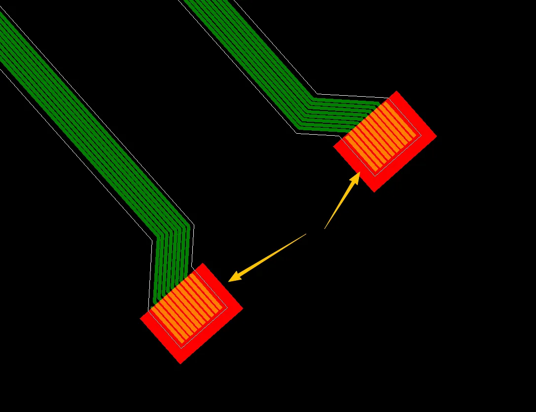
Figure 2: recommend solder mask fully opening at the finger area
Capability Assessment of the Proposed Stackup
The first action was to request complete Gerber data that matched the declared 4-layer construction. Without a verified fourth copper layer the stackup thickness calculation, impedance (if any), and plating balance could not be confirmed. Once corrected files arrived, the stackup was reconstructed as a hybrid build: rigid FR-4 core with flex polyimide laminated to one outer surface. Inner copper was set at 0.5 oz (½ oz) and outer copper at 1 oz, consistent with the process note.
Lamination capability was evaluated against the ±0.1 mm overall tolerance. For a 1.0 mm finished board the press cycle must control resin flow, temperature ramp, and pressure uniformity across both rigid and flex regions simultaneously. The flex material SF305C has a lower resin content and different flow behavior than the FR-4 prepreg. Consequently the press recipe was adjusted for a slower ramp and extended hold time to equalize thickness. Cross-section measurements on first-article panels confirmed that the 1.0 ± 0.1 mm window and the 0.2 ± 0.05 mm flex thickness were both repeatable.
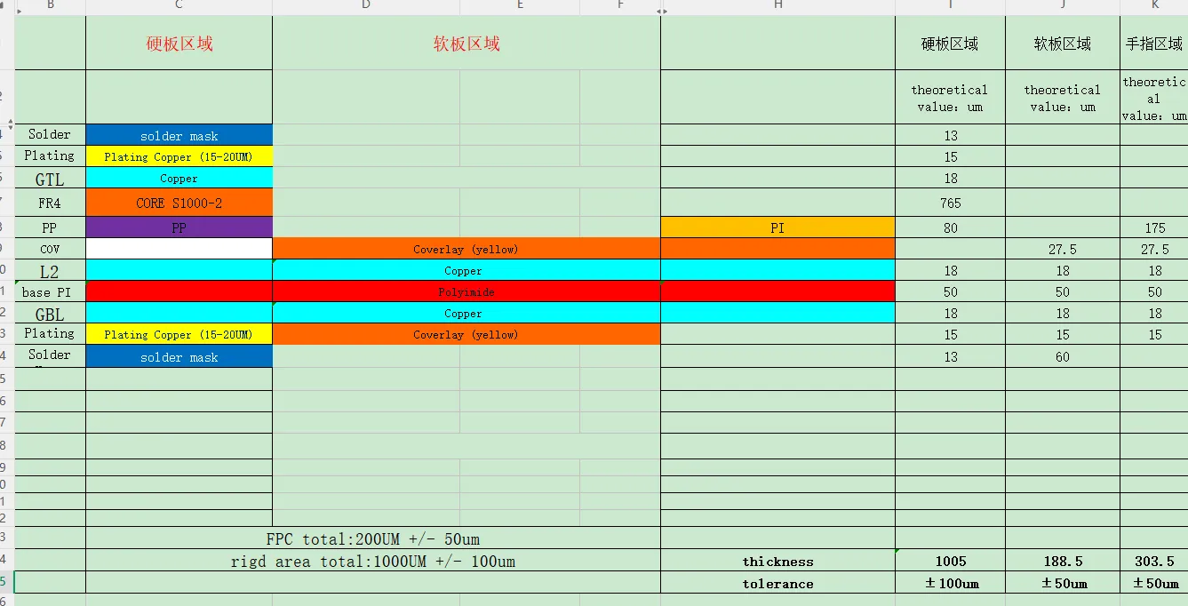
Figure 3: our lamination stack-up
Warpage control relied on three practical measures. First, copper density was balanced as far as the artwork allowed by adding non-functional copper pours on the rigid side opposite the flex. Second, the panel was cooled under restraint after lamination. Third, the finished boards were measured against a flat reference; any units exceeding 2 % were rejected. These steps kept the process inside the accepted limit without requiring a redesign to a symmetrical stackup.
| Process Step | Control Parameter | Target | Observed Result |
|---|---|---|---|
| Lamination | Thickness uniformity | 1.0 ± 0.1 mm | Within ±0.08 mm |
| Cooling under load | Warpage | ≤ 2 % | 1.4–1.9 % |
| PI stiffener placement | Edge registration | ≤ 0.2 mm overhang | Verified by AOI |
| Finger thickness | Final stack height | 0.3 ± 0.05 mm | 0.28–0.32 mm |
Stiffener Geometry and ZIF Finger Reliability
The customer specified that PI stiffeners of 0.1 mm thickness appear only on the two flex tails measuring 5.5 mm by 4.425 mm. When the stiffener outline is cut identically to the gold-finger copper, the insertion force of a ZIF connector is transmitted directly into the adhesive interface and the thin flex copper. Process experience shows that such equal-size stiffeners raise the probability of finger fracture after a few dozen mating cycles.
Engineering therefore recommended two adjustments that remain inside the original design envelope. First, a solder-mask gang opening was applied over the entire finger area so that the ENIG surface remained fully accessible and free of mask residue. Second, the PI stiffener was kept slightly shorter than the copper pads at the free end, creating a short unsupported copper zone that absorbs bending stress. These changes do not alter the overall thickness target of 0.3 ± 0.05 mm yet measurably improve mechanical durability.
No process edge or multi-up panelization was requested. The single-piece outline therefore required careful routing and laser profiling at the flex contours. The absence of a process edge removed one common source of handling stress, but it also meant that all dimensional references had to be taken from the finished outline itself. Optical measurement after final routing confirmed that the flex-tail dimensions and stiffener locations remained within the stated tolerances.
Validation of Process Capability
First-article panels were subjected to cross-section analysis at the rigid-to-flex transition, the finger zone, and the mid-board rigid section. Thickness measurements confirmed the 1.0 ± 0.1 mm overall, 0.2 ± 0.05 mm flex, and 0.3 ± 0.05 mm finger targets. Micro-sections also verified that the PI stiffener edge registration stayed inside 0.2 mm and that no delamination or resin voids were present at the hybrid interface.
Warpage was measured on a flat granite surface with feeler gauges at multiple points. All boards fell between 1.4 % and 1.9 %, satisfying the 2 % acceptance criterion. Electrical continuity and isolation testing across the five pieces showed no opens or shorts attributable to the asymmetrical construction or the stiffener placement.
These results demonstrated that the asymmetrical rigid-flex PCB stackup design, once the copper-layer data were corrected and the process controls were applied, remained inside a stable manufacturing window. The combination of balanced copper, controlled lamination cooling, precise stiffener registration, and open-window solder mask at the fingers converted an initially borderline capability request into a repeatable production process.
Conclusion
The engineering evaluation established that an asymmetrical rigid-flex PCB stackup with 1.0 ± 0.1 mm overall thickness, 0.2 mm flex tails, and localized 0.1 mm PI stiffeners can be manufactured reliably when three conditions are met: complete and consistent layer data, active warpage-control measures during lamination and cooling, and careful stiffener-to-finger geometry that avoids equal-size stress concentration. The final process window delivered boards meeting both the dimensional tolerances and the 2 % warpage limit while preserving the mechanical integrity required for ZIF connector use.
This case illustrates that rigid-flex PCB stackup design decisions must be evaluated against actual process capability rather than nominal material thicknesses alone. When the physical limits of differential expansion, copper-weight transition, and local stiffness are quantified and controlled, even an asymmetrical construction can be released for production with predictable yield and performance.
FAQ
Q1: Why does an asymmetrical rigid-flex stackup increase warpage risk?
A1: The flex polyimide and FR-4 rigid materials expand and contract at different rates. When the flex is placed on only one side, residual stress after cooling produces a measurable bow. Typical uncontrolled asymmetrical builds can exceed 2–3 % warpage; controlled cooling and copper balancing keep the value inside a 2 % acceptance window.
Q2: How tight can overall thickness tolerance be held on a hybrid rigid-flex board?
A2: A ±0.1 mm tolerance on a 1.0 mm finished thickness is achievable with modern presses, but the process window is narrow. Resin flow differences between FR-4 and polyimide require adjusted press recipes and post-lamination verification. Wider tolerances (±0.13 mm or greater) are preferred for high-volume runs.
Q3: Why should PI stiffeners not match the exact outline of gold fingers?
A3: When the stiffener edge coincides with the copper pad edge, insertion and extraction forces concentrate at a single interface. A short unsupported copper zone at the free end distributes bending stress and reduces the likelihood of fracture after repeated ZIF mating cycles.
Q4: What is the practical thickness control for the finger zone on a 0.2 mm flex?
A4: Adding a 0.1 mm PI stiffener yields a nominal 0.3 mm stack. With careful adhesive and coverlay control the finished thickness can be held to ±0.05 mm. Registration of the stiffener edge relative to the copper must be verified optically to stay inside that window.
Q5: How does copper weight difference between rigid and flex regions affect manufacturability?
A5: Different starting copper weights produce different etch and plating rates. The transition zone can develop local thickness steps that become stress risers. Balanced non-functional copper and controlled plating current density minimize the step height and improve long-term reliability of the rigid-to-flex interface.
Q6: Is a 2 % warpage limit realistic for production of asymmetrical rigid-flex boards?
A6: Yes, provided copper balancing, restrained cooling, and 100 % post-process measurement are applied. Without those controls the same construction frequently exceeds 2.5 %. The 2 % figure therefore represents a controlled process capability rather than a free design allowance.
```






