










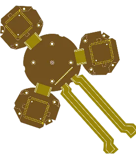
PCB Specifications
| Parameter | Value | Parameter | Value |
|---|---|---|---|
| PCB Type | Rigid-Flex PCB | Quantity | 5 pcs |
| Layers | 4 Layers | Board Type | Single PCB |
| Dimensions | 119.87 x 109.66 mm | Copper Weight | 1OZ |
| Thickness | 1 mm | Min Track / Spacing | 6/6mil↑ |
| Surface Finish | ENIG (Immersion Gold) | Min Hole Size | 0.3mm↑ |
| Solder Mask | Green | Silkscreen | White |
Manufacturing Timeline
Logistics Information
Key Manufacturing Processes
Manufacturing Summary
This rigid-flex PCB was produced as a 4-layer construction with overall dimensions of 119.87 × 109.66 mm and a finished thickness of 1.0 mm. The rigid sections used FR-4 (Shengyi S1150G, TG155) with 1 oz copper, while the flex sections were 2-layer polyimide (Shengyi SF305C) at 0.2 mm thickness with 1/3 oz inner and 1 oz outer copper. Surface finish was ENIG, solder mask green on rigid areas and yellow on flex, with white silkscreen. Quantity was limited to 5 pieces in single-piece form, processed with combined mechanical routing and laser profiling, and verified by full flying-probe testing within the 18-day lead time.
Key engineering clarifications addressed incomplete Gerber layer data (G1 empty and G2 incomplete despite the 4-layer designation) before stackup finalization. The outer-layer flex placement created an asymmetric structure, so 2% board warpage was accepted as a normal outcome. PI stiffeners measuring 5.5 × 4.425 mm were applied only on the two flex tails; because the PI matched finger dimensions, open-window treatment at the contact fingers was recommended and implemented to reduce insertion stress and prevent fracture risk. Stackup targets were locked at total thickness 1.0 ± 0.1 mm, flex 0.2 ± 0.05 mm, and finger region 0.3 ± 0.05 mm with 0.5 oz inner copper.
All adjustments were confirmed and executed, resulting in consistent layer registration, controlled warpage within the accepted limit, and intact finger integrity after forming. Detailed records of the asymmetric rigid-flex stiffener and finger stress control applied to this order provide further reference for similar constructions.
Explore More PCB Manufacturing Resources
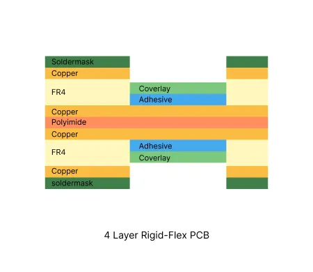
4 Layer Rigid-Flex PCB Manufacturing Insights
Discover how AIVON manufactures 4 Layer Rigid-Flex PCBs, including rigid and flexible layer integration, mechanical reliability requirements, fabrication processes, manufacturing challenges, and real production experience from customer orders.
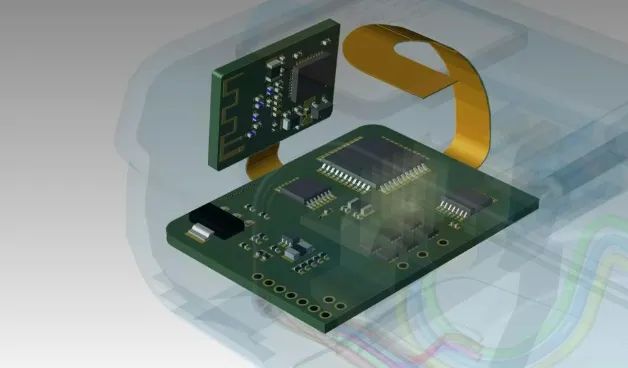
The Ultimate Guide to Rigid-Flex PCB Design: Mastering Reliability, Complexity, and Cost
Master the complexities of Rigid-Flex PCB Design with this 2,500-word guide. Explore stack-up symmetry, bend radius calculations, via optimization, and cost-effective manufacturing strategies.
Real Production Records
| Order ID | PCB Type | Layers | Dimensions | Solder Mask | Surface Finish | Quantity | Action |
|---|---|---|---|---|---|---|---|
| RFP-20260723-038 | Rigid-Flex PCB | 4 | 186 x 111.6 | Green | ENIG (Immersion Gold) | 10 | View detail |
| RFP-20260626-0002 | Rigid-Flex PCB | 4 | 100 x 106.01 | Green | ENIG (Immersion Gold) | 5 | View detail |
| RFP-20260608-0005 | Rigid-Flex PCB | 4 | 22.15 x 97.92 | Green | ENIG (Immersion Gold) | 20 | View detail |


