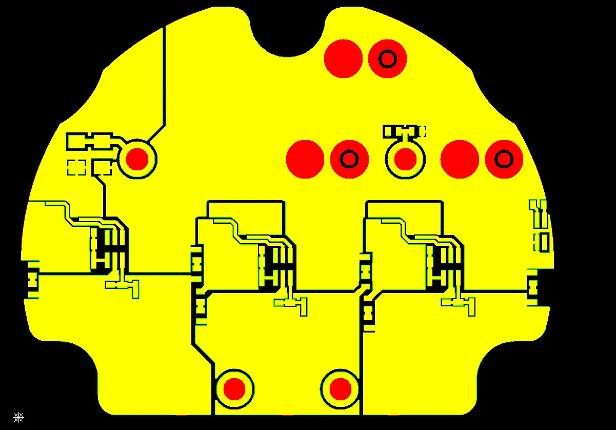
A 4-layer FR-4 board measuring 22 mm × 45.5 mm entered CAM review as a factory-panelized 4 × 2 array with 4 mm process edges on the top and bottom sides. The order specified TG150 material, 0.8 mm thickness, 1 oz copper on all layers, green solder mask on both sides, no silkscreen, immersion gold (ENIG) with 3 µin gold thickness, via tenting, V-cut separation, and 100 % flying-probe testing. Quantity was 120 pieces across 15 sets. The customer note explicitly required sequential ID numbers on each PCB within the panel, marked left-to-right and top-to-bottom on the solder resist mask in accordance with IPC-4552 recommendations for ENIG, without reducing clearance. During data verification the absence of any character (silkscreen) layer, combined with limited free space on the solder-mask layers, made it impossible to place the required serial numbers and UL marks in the locations originally indicated. The investigation therefore focused on establishing a manufacturable marking method that satisfied both the IPC-4552 intent and the physical constraints of the small board.
Design Intent for Sequential ID and UL Marking
The customer's board ( #FR4-20260505-022 ) fabrication note and the accompanying IPC-4552 reference made clear that every individual board on the panel needed a unique sequential identifier printed on the solder-mask surface. The note further stipulated that the marking must not reduce electrical clearance. In parallel, a UL mark was requested. On a board only 22 mm × 45.5 mm, free copper-free or mask-open areas large enough for legible characters are scarce. The design files contained no silkscreen layer at all, so the only available surface for permanent identification was the solder mask itself. The apparent intent was therefore to use solder-mask legend for both the sequential serial numbers and the UL symbol while preserving the existing clearance rules and the ENIG finish integrity.
Missing Character Layer and Insufficient Mask Space
Our CAM engineer first confirmed that the Gerber package contained no character layer. Serial numbers and UL marks can normally be placed on silkscreen; when that layer is absent the only remaining option is to add a new silkscreen layer for the sequential ID number. Examination of the top and bottom solder mask layers showed that the positions originally indicated for the serial numbers and the UL box lacked sufficient clear area. On the bottom side the free space was especially constrained; the requested UL location could not accommodate the required symbol size without overlapping copper or reducing clearance. On the top side a nearby LMP marking occupied a usable pocket of mask, creating a potential swap opportunity.
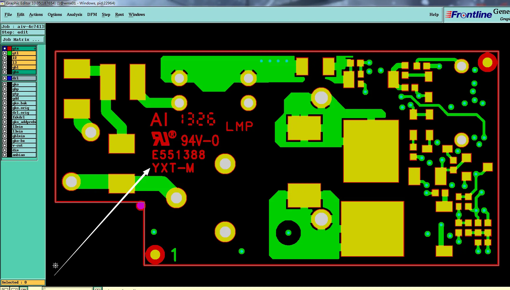
Figure 1: add ul to the top layer solder mask
If the markings had been forced into the original locations, two realistic manufacturing risks would have arisen. First, the text or UL box would have encroached on copper features, violating the customer's own clearance requirement and potentially creating solder-mask dams thinner than process capability. Second, characters printed on an overcrowded mask area can become illegible after ENIG and final cure, defeating the traceability purpose of the sequential ID. Either outcome would have rendered the boards non-compliant with the stated IPC-4552 intent and with basic identification needs.
| Marking Requirement | Original Location Status | Space Constraint | Risk if Forced |
|---|---|---|---|
| Sequential ID (IPC-4552) | No silkscreen layer present | Specified positions too small | Illegible or clearance violation |
| UL mark on bottom SM | Requested bottom location | No usable free area | Overlap or missing mark |
| UL box size | Indicated pocket too narrow | Cannot fit required symbol | Incomplete or unreadable UL |
Marking Placement Without Silkscreen or Adequate Space
The dominant conflict belonged to the combined categories of documentation conflict and design-intent ambiguity. The customer required sequential identification on the solder-mask surface per IPC-4552, yet the design files supplied neither a character layer nor sufficient clear mask area at the indicated coordinates. On a board only 22 mm wide, every square millimeter of mask is already allocated to functional openings or copper protection. Adding text or a UL symbol therefore required either relocating existing features or accepting a reduction in clearance—both of which contradicted the written note.
Because the panel was factory-generated in a 4 × 2 array, the sequential numbering also had to follow a consistent left-to-right, top-to-bottom order across the entire panel. Without confirmed locations the CAM system could not generate the mask artwork that simultaneously satisfied traceability, UL identification, and clearance rules. Production release was therefore blocked until the customer authorized alternative placement coordinates that preserved electrical clearance and remained legible after ENIG processing.
Supporting Observations on Panel and Mask Constraints
Secondary observations reinforced the space problem. The 0.8 mm board thickness and 4 × 2 panel format with only 4 mm process edges left limited real estate outside the functional circuitry. Via tenting further reduced the continuous mask areas available for legend. The bottom-side mask in particular offered no pocket large enough for the UL symbol, while a usable region existed on the top side near an existing LMP marking. These facts made a simple "add the mark where indicated" solution impossible and confirmed that relocation or swapping was the only practical path.
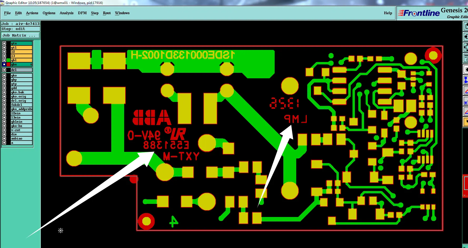
Figure 2: swap positions with LMP
Relocation of Serial ID and UL Marks on Solder Mask
The engineering proposal contained three coordinated adjustments. First, because no character layer existed, we advise adding a new silkscreen layer for the sequential ID number, at the location shown in the image. Second, the sequential ID numbers would be placed in the nearest available clear mask regions that still allowed left-to-right, top-to-bottom ordering across the 4 × 2 panel without reducing clearance. Third, the UL mark, originally requested on the bottom side, would be moved to a verified open area on the top solder mask; where the indicated UL box was too small, its position would be swapped with the adjacent LMP marking so that both features retained adequate size and legibility.
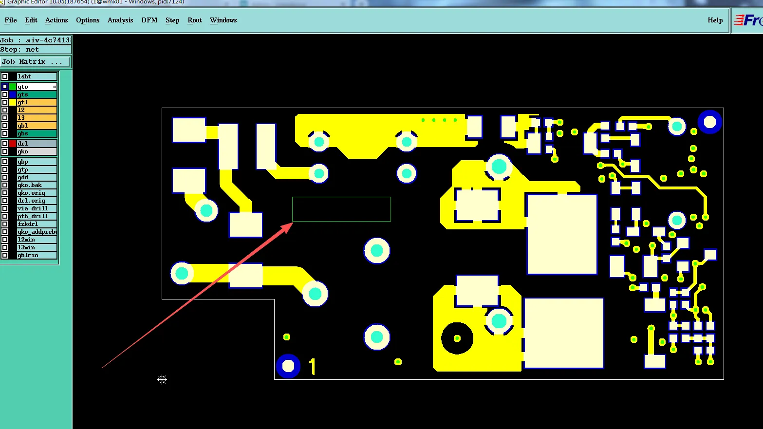
Figure 3: adding a new silkscreen layer for the sequential ID number, at the location shown in the image
Customer confirmation accepted the relocation of the serial numbers and the transfer of the UL mark to the top solder-mask layer, including the LMP swap. The solder-mask Gerbers were regenerated with the new legend locations, clearance was re-verified against the copper layers, and the sequential numbering scheme was locked to the panel array. With the marking conflict resolved, the remaining file-confirmation steps were closed and the 15-set order was released for production.
| Engineering Observation | Conflict Identified | Recommended Action | Final Status |
|---|---|---|---|
| No character layer in Gerber package | Serial numbers cannot be placed on silkscreen | adding a new silkscreen layer for the sequential ID number | Implemented |
| Specified serial positions lack space | Clearance or legibility risk | Relocate to nearest clear mask areas | Confirmed |
| Bottom SM has no room for UL | UL mark cannot fit as requested | Move UL to top SM, swap with LMP if needed | Implemented |
| UL box pocket too small | Symbol would be incomplete | Exchange position with LMP marking | Confirmed |
Design Lessons for Marking on Small ENIG Boards
- When sequential ID numbers are required on solder mask per IPC-4552, provide either a character layer or explicitly designated clear mask areas large enough for the text.
- On boards smaller than approximately 30 mm in any dimension, verify free mask space before specifying mark locations; overcrowding forces relocation or clearance violations.
- If a UL or other regulatory mark is mandatory, confirm that the chosen side and coordinates can accommodate the full symbol size without overlapping copper.
- Absence of a silkscreen layer does not eliminate marking requirements; it simply moves the legend into the solder-mask artwork and tightens space constraints.
- Factory-panelized arrays that need left-to-right, top-to-bottom numbering must have consistent, pre-approved locations so the sequential scheme can be generated automatically.
- Swapping an existing mark (such as LMP) with a required UL or serial feature is often the cleanest solution when the original pocket is too small.
- Always re-check electrical clearance after any legend is added to the solder-mask layer; the customer note itself forbids reduction of clearance.
FAQ
Q1: Why can't sequential ID numbers be placed when no silkscreen layer exists?
A1: Silkscreen is the normal carrier for legend. Without it the only permanent surface is the solder mask, which must already contain sufficient clear area at the chosen coordinates.
Q2: What happens if a required mark is forced into a location that is too small?
A2: The characters become illegible or the mask encroaches on copper, violating clearance rules and potentially creating solder-mask bridges thinner than process capability.
Q3: Why does IPC-4552 matter for ENIG boards?
A3: IPC-4552 provides recommendations for marking and identification on immersion-gold finishes. The customer explicitly invoked those recommendations for sequential panel numbering.
Q4: Can a UL mark be moved from the bottom to the top solder-mask layer?
A4: Yes, provided the customer confirms the new location and the top-side mask still offers adequate clear area and clearance.
Q5: Why is swapping an LMP mark with the UL box a practical solution?
A5: It re-uses an already clear mask pocket of sufficient size, avoiding the need to create new open areas or reduce copper clearance.
Q6: How should designers prepare small boards that require both serial numbers and UL marks?
A6: Either supply a dedicated character layer or pre-allocate and document clear solder-mask regions large enough for every required legend element before the files are released for CAM.