










During CAM review of a thin 4-layer FR-4 board measuring 418 mm by 38 mm with extremely high hole density, our engineering team identified multiple locations where the designed solder-mask dams between fine-pitch IC pads fell below reliable manufacturing limits. From a DFM perspective, the primary concern was manufacturing stability and the prevention of solder bridging during SMT assembly. Without clarification, the finished boards could have entered production with missing or broken solder-mask bridges, allowing molten solder to short adjacent pads and generating high assembly reject rates. This case provides practical insight into PCB Solder Mask Bridge Minimum Width requirements for high-density, fine-pitch designs.
The order ( #FR4-20260105-006 ) specified FR-4 (KB-6160), TG130, 0.8 mm thickness, 1 oz copper on all layers, green solder mask on both sides, white silkscreen, immersion gold finish at 1 µin with 20 % gold area, single-piece shipment with no process edge, 100 % flying-probe testing, and a five-day delivery window. Quantity was 300 pieces. These parameters are typical for compact, high-density modules, yet the combination of ultra-fine IC spacing, high hole density exceeding 470 000 per square meter, and thin 0.8 mm construction required explicit engineering confirmation before release.
Why Fine-Pitch Mask Dams Triggered Immediate DFM Scrutiny
Our CAM engineer first examined the solder-mask layer against the outer copper pads, particularly around fine-pitch IC footprints. In several locations the gap between adjacent pads measured less than 0.18 mm. At this distance it is no longer possible to retain a stable solder-mask dam (bridge) during imaging, development, and curing. The mask either breaks or is deliberately removed, leaving a continuous opening that allows solder to flow freely between pads during reflow.
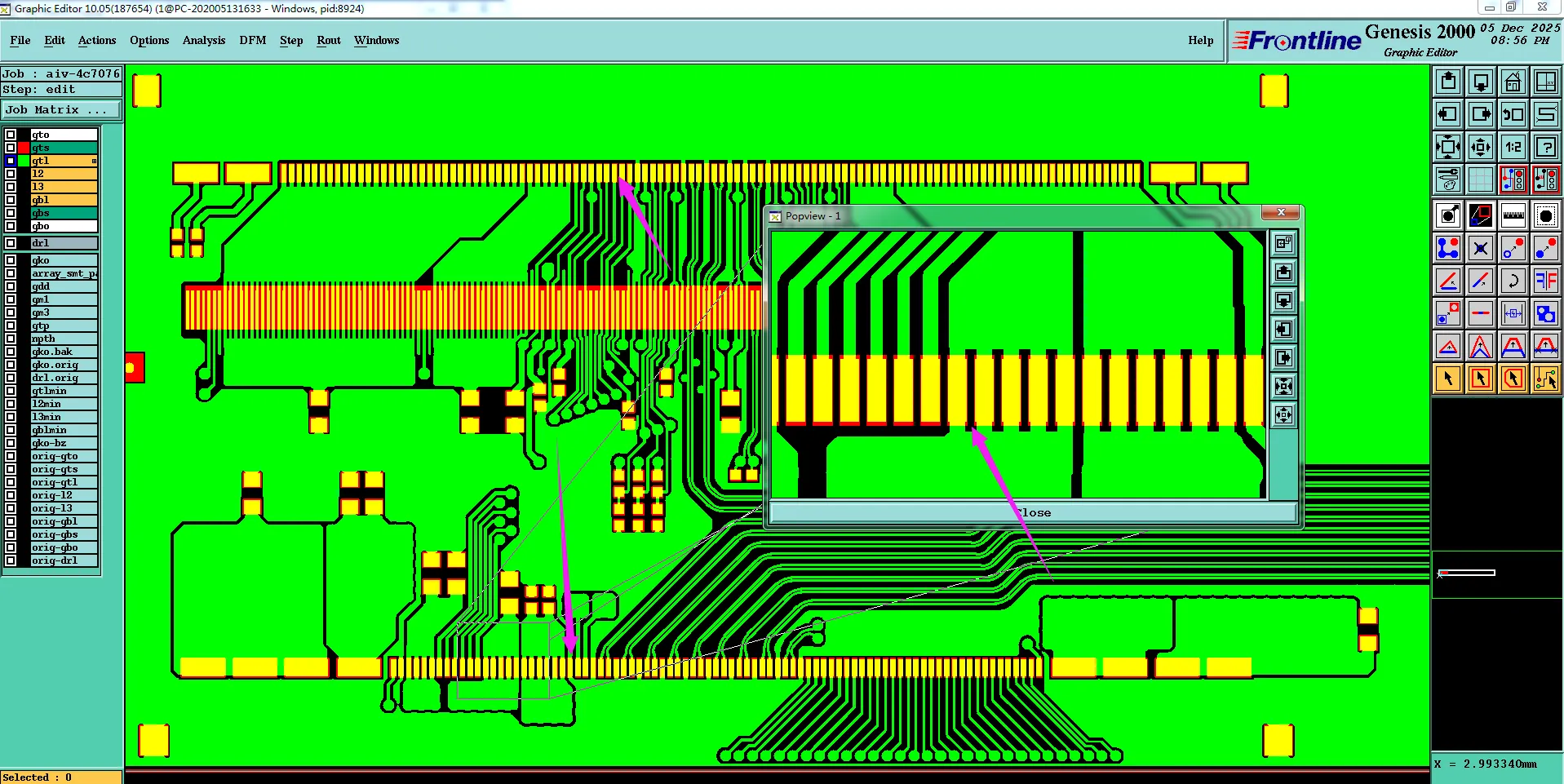
Figure 1: the original IC pad-to-pad spacing is less than 0.18mm
Additional observations included solder-mask openings that crossed the center of individual pads (creating an internal dam that could not be retained), silkscreen characters whose height and width fell below the practical minimum for legible printing, non-functional isolated pads on inner layers, and fabrication notes that the factory would ignore for production. These secondary items added complexity, but the insufficient solder mask bridge width remained the highest-risk issue for assembly yield.
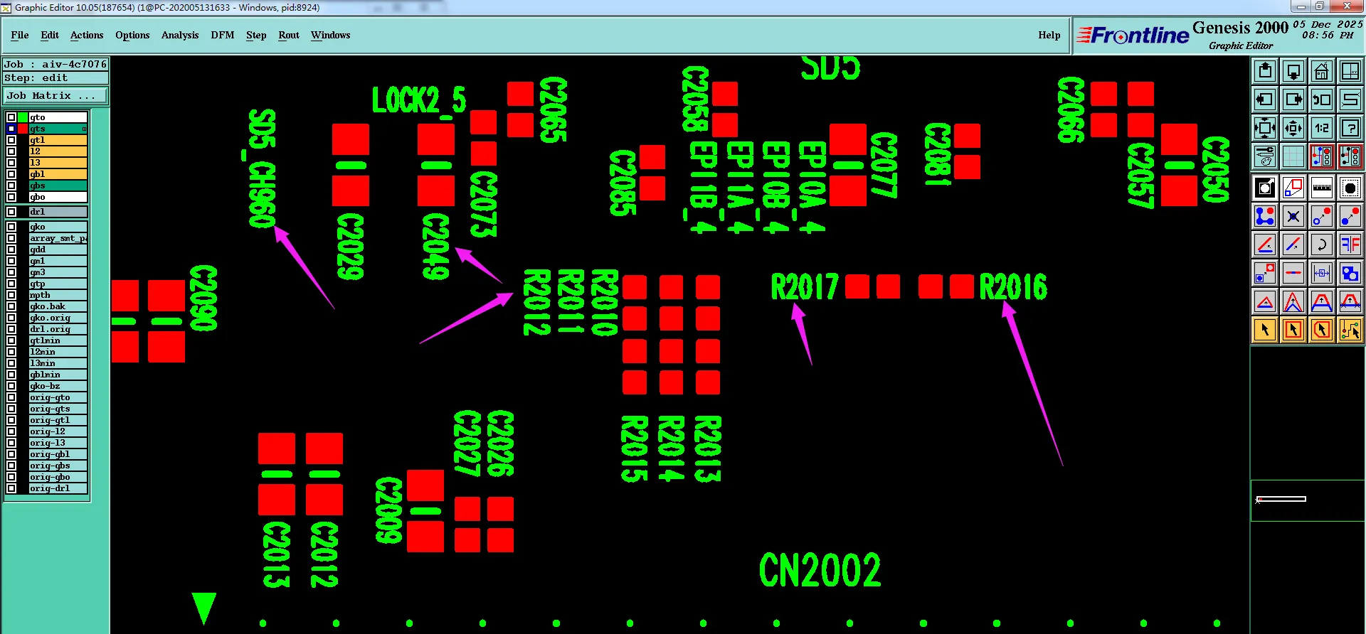
Figure 2: the character height and width are insufficient
Risk indicators included the extremely high hole density, the thin 0.8 mm core, the long narrow board geometry, and the presence of fine-pitch ICs whose pad-to-pad gaps approached or fell below the process capability for green solder mask. On such boards any missing dam directly translates into solder bridges that fail visual and electrical inspection after SMT.
| Feature Observed | Condition in Files | Primary DFM Risk |
|---|---|---|
| IC pad-to-pad spacing | Less than 0.18 mm | No reliable solder-mask bridge |
| Pad with central mask opening | Internal dam cannot be retained | Uncontrolled solder flow |
| Silkscreen character size | Below 0.75 mm height / 0.65 mm width | Blurred or incomplete legend |
Table 1 summarizes the key observations that generated the Engineering Question.
Narrow Solder Mask Bridges and Related Surface Risks Identified
The dominant risk was the inability to retain solder-mask dams between fine-pitch IC pads whose spacing measured less than 0.18 mm. When the designed gap is too narrow, the mask either fractures during processing or must be removed entirely, converting individual pad openings into a single gang opening. Molten solder can then bridge adjacent pads during reflow, creating short circuits. A second risk involved pads that carried a solder-mask opening across their center; the resulting internal dam could not be preserved, again allowing uncontrolled solder flow. A third observation concerned silkscreen characters that fell below the practical minimum size, risking illegible or incomplete markings after printing.
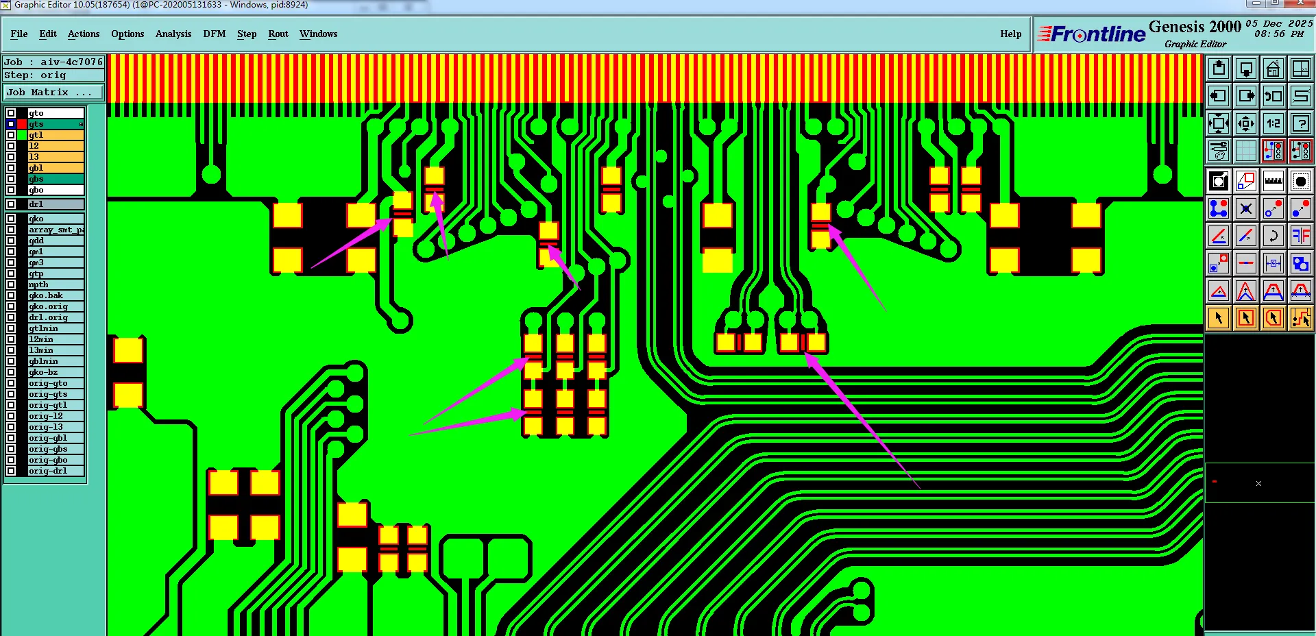
Figure 3: a solder mask opening designed between the pads
Secondary items included non-functional isolated pads on the inner layers (recommended for deletion to simplify fabrication) and fabrication notes that would be ignored during production. These required confirmation but did not carry the same immediate assembly-critical weight as the solder-mask bridge limitations.
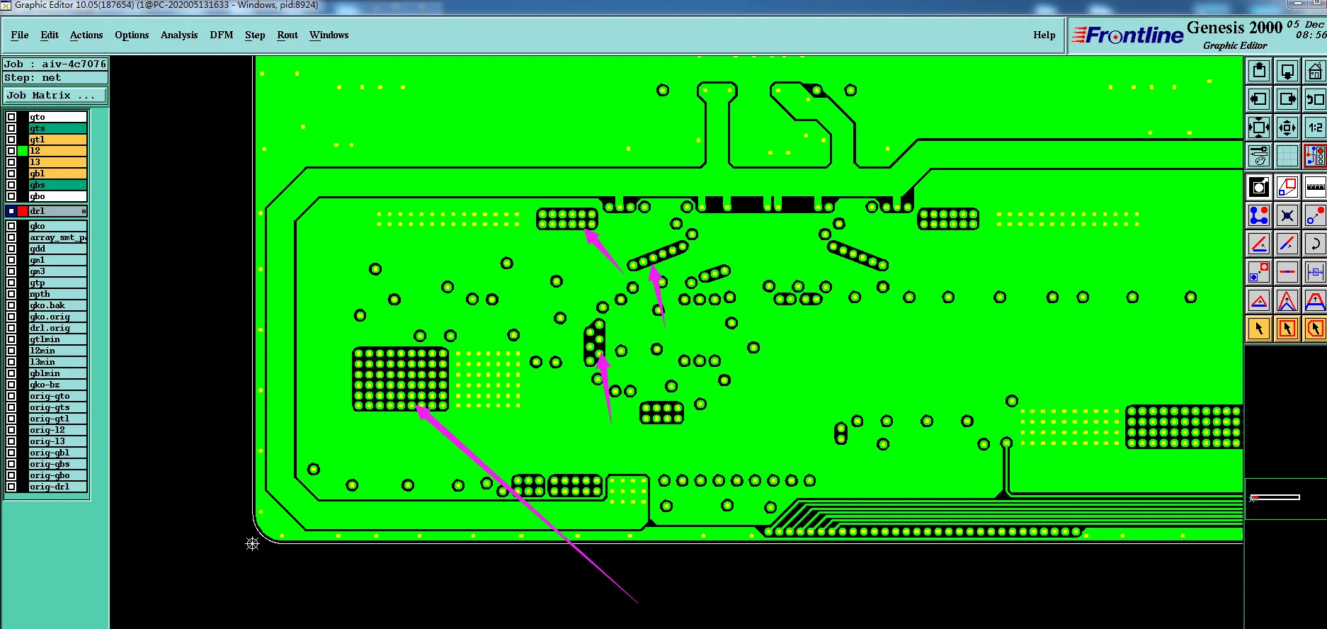
Figure 4: non-functional isolated pads on the inner layers
From a DFM perspective the priority sequence was clear: decide whether to open the fine-pitch areas fully or accept the loss of dams, clarify the treatment of central pad openings, and document the remaining cosmetic and inner-layer adjustments before any tooling was released.
How Missing Solder Mask Bridges Threaten Assembly Yield and Reliability
If production had continued without addressing the narrow mask dams, the finished boards would have arrived at SMT assembly with continuous openings between fine-pitch pads. During reflow the solder paste would form bridges, producing short circuits that fail automated optical inspection or functional test. Even if some bridges were manually reworked, the residual risk of intermittent shorts under thermal cycling would remain. On a thin 0.8 mm board with high hole density these defects also increase the chance of localized stress and long-term joint degradation.
According to common IPC-2221 spacing guidance and practical solder-mask process capability, a minimum dam width is required to ensure the mask survives imaging and curing. When the designed gap falls below this threshold the dam cannot be guaranteed, and the design must either be modified or the opening accepted as a gang window. Based on IPC-A-600 acceptability considerations, solder bridges between adjacent pads are classified as defects that directly impact electrical performance and customer acceptance.
Central openings within individual pads create a similar uncontrolled solder path. Silkscreen characters below the recommended 0.75 mm height and 0.65 mm width become blurred or incomplete, reducing traceability and risking cosmetic rejects. Non-functional inner pads, if left in place, add unnecessary etching complexity without contributing to electrical function.
| Potential Failure Mode | Root Cause Linked to EQ | Production or Field Impact |
|---|---|---|
| Solder bridges between IC pads | Pad gap < 0.18 mm, no dam | SMT short circuits, high reject rate |
| Uncontrolled solder flow on pads | Central mask opening on pad | Incomplete joints or shorts |
| Illegible silkscreen | Character size below minimum | Cosmetic rejects, traceability loss |
| Unnecessary inner-layer features | Non-functional isolated pads | Added process complexity |
Table 2 maps each realistic failure mode to the Engineering Question items.
Failure Scenarios the Engineering Team Sought to Prevent
Had the original fine-pitch mask dams remained, boards reaching the SMT line would have shown continuous openings between adjacent IC pads. Solder paste would form bridges during reflow, producing short circuits that fail AOI or functional testing. Manual rework of hundreds of fine-pitch bridges is impractical under a five-day schedule and often leaves residual reliability concerns. On a thin, high-density board these shorts can also create localized heating that accelerates long-term joint degradation.
Leaving central openings within individual pads would have allowed solder to flow in uncontrolled patterns, potentially starving the joint of solder or creating unwanted connections. Silkscreen characters printed below the minimum size would have appeared blurred or incomplete, generating cosmetic rejects and reducing the ability to identify boards in the field. Non-functional inner pads, if retained, would have added etching complexity without any electrical benefit.
All of these scenarios share a common origin: insufficient design-for-manufacturing margin at the solder-mask and legend interfaces on a fine-pitch, high-density board.
Preventive Actions Confirmed During the DFM Exchange
Our engineering team issued a focused Engineering Question that first addressed the fine-pitch IC areas. Because the pad-to-pad spacing measured less than 0.18 mm, it was impossible to retain a reliable solder-mask dam. The recommendation was to open these areas fully (gang opening) so that the mask process would be stable and the customer would understand that no dam would be present. The customer accepted this approach.
For pads that carried a central solder-mask opening the team confirmed that an internal dam could not be preserved and requested guidance on whether to follow the original design or adjust the opening. Non-functional isolated pads on the inner layers were proposed for deletion to simplify fabrication; the customer accepted the removal. Silkscreen characters below the practical minimum of 0.75 mm height and 0.65 mm width were flagged, and the customer was asked to accept possible blurring or incompleteness. Fabrication notes shown in the artwork were documented as ignored during production.
With these decisions locked, the CAM data were updated, the fine-pitch areas were converted to full openings, non-functional inner pads were removed, and the order was released under the five-day schedule. The revised design retained all electrical functionality while eliminating the primary sources of solder bridging and surface defects.
| Action Item | Customer Decision | Manufacturing Benefit |
|---|---|---|
| Fine-pitch IC mask dams | Full opening accepted | Stable mask process, no broken dams |
| Central pad openings | Design intent confirmed | Clear solder-mask treatment |
| Non-functional inner pads | Deletion accepted | Simplified inner-layer etching |
Table 3 records the closed-loop decisions that converted a high-risk fine-pitch design into a manufacturable product.
Building Trust Through Early Mask-Bridge Verification
This case demonstrates that solder-mask dam width is not a minor cosmetic detail on fine-pitch, high-density boards; it is a direct determinant of SMT yield and long-term reliability. By identifying the gaps below 0.18 mm during CAM review and obtaining explicit customer acceptance of full openings, the engineering team protected both first-pass assembly success and the five-day delivery commitment. Documentation of silkscreen limits, inner-pad deletion, and ignored notes further reduced the chance of late-stage surprises.
Designers working with fine-pitch ICs on thin FR-4 boards are encouraged to maintain pad-to-pad gaps compatible with the chosen solder-mask process, avoid internal dams that cannot be retained, keep silkscreen characters above the practical minimum size, and request early DFM feedback on mask-bridge feasibility. These practices convert potential manufacturing and assembly problems into controlled, documented decisions before production begins.
Proactive verification of PCB Solder Mask Bridge Minimum Width remains one of the highest-leverage actions a DFM team can take when releasing high-density multilayer boards for SMT assembly.
FAQ
Q1: Why is a minimum solder-mask bridge width required between IC pads?
A1: The solder-mask dam must survive imaging, development, and curing. When the pad-to-pad gap falls below approximately 0.18 mm on standard green-mask processes, the dam cannot be reliably formed and either breaks or must be removed, allowing solder to bridge adjacent pads during reflow.
Q2: What happens if solder-mask dams are missing on fine-pitch ICs?
A2: Molten solder flows freely between pads, creating short circuits that fail AOI or functional testing. Manual rework is difficult and often incomplete, leaving residual reliability risks under thermal cycling.
Q3: Why convert fine-pitch areas to full openings when dams cannot be retained?
A3: A full (gang) opening produces a stable, predictable mask process. Attempting to force a dam that is narrower than process capability creates broken or irregular mask features that are worse than a clean full opening.
Q4: How does silkscreen character size affect manufacturability?
A4: Characters below approximately 0.75 mm height and 0.65 mm width tend to print blurred or incomplete. This reduces legibility and can generate cosmetic rejects, especially on high-density boards with limited free space.
Q5: Why remove non-functional isolated pads from inner layers?
A5: Isolated pads that serve no electrical purpose add etching complexity and potential registration issues without contributing to circuit function. Removing them simplifies fabrication while leaving all functional copper intact.
Q6: How can designers avoid similar solder-mask bridge issues on future boards?
A6: Maintain pad-to-pad gaps compatible with the chosen solder-mask process (typically ≥0.18 mm for standard green mask), avoid internal dams that cannot be retained, keep silkscreen characters above the practical minimum size, and request early DFM review of fine-pitch areas. These steps form the practical foundation of PCB Solder Mask Bridge Minimum Width rules.






