










A high-volume 4-layer FR-4 order with 13,200 pieces arranged as 4,400 sets requires careful production preparation before the manufacturing package can be released. The board measures 280.7 × 166.4 mm, uses TG130 material, 1.6 mm thickness, and 1 oz copper on both sides. Solder mask is green and silkscreen is white on both sides. Surface finish is leaded HASL, vias are tented, and depanelization is by V-cut. The customer specified self-panelization in a 1 × 3 array with zero process edge. In addition, the customer note requested UL certification marking and a date code. The engineering questions focused on confirming the exact 1 × 3 panel layout based on the single-board file and addressing silkscreen characters that fell below process limits. These items formed the core of the production-readiness work.
Our CAM review treated the panelization confirmation as the primary production-preparation activity. Supporting decisions on silkscreen acceptance and the addition of UL and date-code markings were handled as coordinated steps that keep the manufacturing package consistent and free of open holds.
Project Overview and Required Production Preparation
The order ( #FR4-20260520-030 ) called for FR-4 (KB-6160) with TG130, four layers, 1.6 mm finished thickness, and 1 oz copper inner and outer. Minimum hole size was 0.3 mm and minimum trace/space 4 mil. Hole copper thickness was specified at 18 µm. The panel arrangement was customer self-panel 1 × 3 with no process edge (0 mm) and V-cut separation. Electrical test used an engineering test fixture, X-out boards were accepted, and lead time was five days. Factory number AIV-4Y7460189 was assigned, production confirmation was yes, and shipping reports included the electrical test report and quality certificate. Material number update and cycle-mark update were both flagged as required. The customer note explicitly requested addition of UL certification and a date code.
Because the process edge was zero and the customer retained final panel control, the manufacturing package had to follow the single-board file exactly when constructing the 1 × 3 array. Any deviation in board spacing, V-cut placement, or outline registration would create downstream handling and depanelization problems. The silkscreen data also required explicit acceptance of characters that fell below the factory's minimum width and height capability. Finally, the UL mark and date code had to be placed in locations that remained legible after V-cut while satisfying the customer's traceability request.
Confirming the 1 × 3 Customer Self-Panel Layout
The first engineering question asked for confirmation of the panelization method and instructed the team to build the 1 × 3 array strictly according to the single-board file supplied to the customer. With zero process edge, the three boards sit edge-to-edge; the only separation features are the V-cut lines. The CAM engineer therefore extracted the exact outline, copper keep-out, and silkscreen boundaries from the single-board data and replicated them three times with the correct pitch. Any added rail or altered spacing would have violated the customer's self-panel intent and created mismatch with the assembly fixtures the customer already planned.
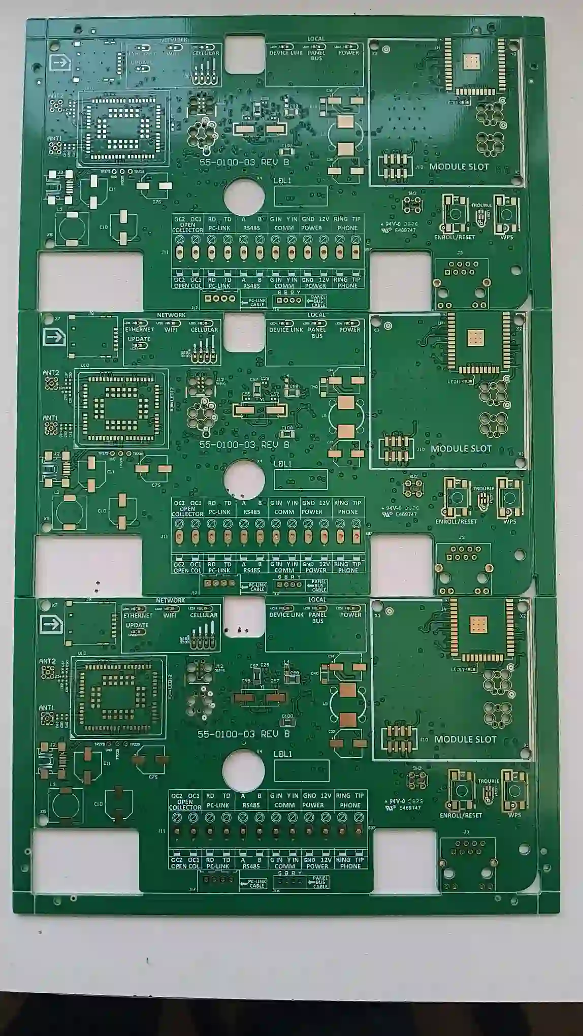
Figure 1: 1 × 3 panel
Once the 1 × 3 geometry was locked, the V-cut depth and residual thickness were calculated against the 1.6 mm board thickness so that the panels would separate cleanly without excessive stress on the 4-layer stack-up. The resulting panel drawing was submitted for customer confirmation. Approval of this drawing eliminated the risk of later disputes over board count per panel, edge quality after breakout, or registration relative to the customer's own tooling.
By fixing the panel layout early, the manufacturing package could proceed to tooling and test-fixture preparation without iterative changes. For a 13,200-piece order the time saved by avoiding panel redesign directly supports the five-day lead time.
Accepting Silkscreen Characters Below Process Limits
The second production-preparation item concerned silkscreen legibility. Several characters in the data measured below the factory's process capability of 0.127 mm width and 0.8 mm height. In addition, portions of the legend overlapped copper pads. Under normal process conditions these features would print incomplete, missing, or blurred. The engineering question therefore asked whether the customer would accept the resulting silkscreen quality if the files were run as-is.
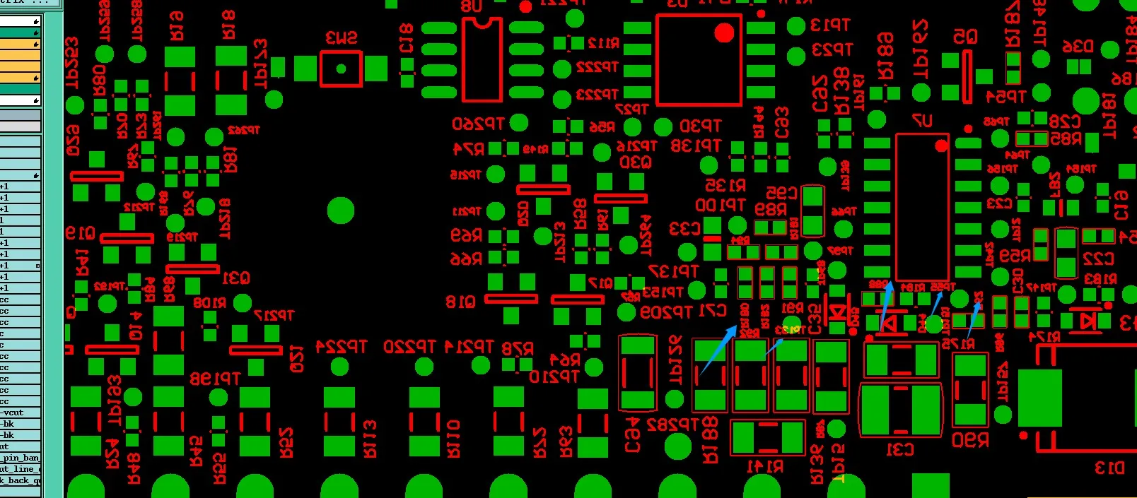
Figure 2: several characters in the data are too small
The customer response was to proceed according to the file and to accept the blurred or incomplete text. This decision removed the need for artwork revision and the associated delay. The CAM engineer documented the acceptance so that quality inspection would apply the correct criteria: characters that fall below process limits are noted but not rejected when the customer has explicitly waived the requirement. The silkscreen plot was released without modification, preserving the original design intent while keeping the production schedule intact.
Documenting the acceptance also protects both parties. Future lots of the same part number can reference the same waiver, avoiding repeated engineering questions and maintaining consistency across the high-volume run.
Adding UL Certification and Date Code Markings
The customer note requested addition of UL certification marking and a date code. Because the process edge was zero, both markings had to be placed on the functional board area in locations that would survive V-cut and remain readable after depanelization. The CAM engineer selected blank silkscreen regions that did not interfere with copper features or component placement. The date code followed the year-week format already flagged for update in the order parameters. The UL mark was positioned according to common practice for permanent identification.
These markings support lot traceability and regulatory identification without requiring extra panel real estate. Once the locations were verified against the single-board file, the silkscreen data were updated and the production draft regenerated. Customer confirmation of the final legend completed the marking package.
With the markings confirmed, the manufacturing package contained every identifier required for quality records and customer receiving inspection. No further silkscreen revisions were needed.
| Engineering Question | Constraint / Root Cause | Resolution |
|---|---|---|
| 1 × 3 self-panel layout | Zero process edge; customer retains panel control | Built strictly from single-board file; V-cut parameters confirmed |
| Silkscreen characters below process limits | Features under 0.127 mm width / 0.8 mm height; some pad overlap | Customer accepted as-is quality; waiver documented for inspection |
| UL mark and date code | No process edge for placement; traceability required | Added in verified blank silkscreen locations; year-week format used |
Table 1: Summary of Production-Preparation Engineering Questions and Resolutions
The Optimization Strategy: High-Volume Efficiency with Zero Process Edge
Confirming the 1 × 3 layout from the single-board file allowed the factory to use the customer's own panel geometry for all subsequent process steps. Tooling holes and test-fixture pins could be referenced directly to the customer's data, eliminating secondary registration steps. The zero-process-edge design maximized material utilization across the 13,200-piece quantity while the V-cut parameters were tuned once and applied uniformly.
Acceptance of the marginal silkscreen characters removed an entire revision cycle. The UL and date-code additions were executed in the same silkscreen update, so only one legend plot was required. The resulting manufacturing package therefore contained a single, self-consistent set of files: the confirmed 1 × 3 panel, the original copper and mask data, the accepted silkscreen (with added markings), and the production draft. This package could be released directly to the five-day production window without further engineering intervention.
Because the panel geometry matched the customer's self-panel intent, downstream assembly handling remained unchanged. The factory's role stayed limited to fabrication and the agreed test method, preserving the efficiency gains of customer-controlled depanelization.
Production Readiness Checklist
Before the manufacturing files were released, the following items were verified against the resolved engineering questions:
- 1 × 3 panel layout constructed strictly from the customer single-board file and confirmed.
- V-cut parameters set for clean separation of the zero-process-edge array.
- Silkscreen characters below 0.127 mm width / 0.8 mm height accepted as-is per customer waiver.
- UL certification mark and year-week date code added in verified silkscreen locations.
- Material-number and cycle-mark updates incorporated.
- Final production draft cross-checked and released for the five-day lead time.
| Check Item | Verification Action |
|---|---|
| Panel layout | Confirm 1 × 3 array built strictly from customer single-board file |
| V-cut parameters | Set depth and residual thickness for clean separation of zero-process-edge boards |
| Silkscreen limits | Document customer acceptance of characters below 0.127 mm width / 0.8 mm height |
| UL and date code | Add both markings in verified silkscreen locations that survive V-cut |
| Material and cycle marks | Incorporate required material-number and cycle-mark updates |
| Final package | Cross-check production draft and release for the five-day lead time |
Table 2: High-Volume Production Readiness Checklist
Final Production Outcome
The engineering preparation converted a high-volume 4-layer design into a production-ready manufacturing package that respected the customer's self-panel geometry, accepted the existing silkscreen limitations, and incorporated the requested UL and date-code markings. Confirmation of the 1 × 3 layout eliminated geometry mismatches. Explicit acceptance of marginal characters removed revision delay. Addition of the permanent identifiers satisfied traceability requirements without extra panel space. The complete package therefore moved directly into fabrication on the five-day schedule, supporting both the large quantity and the customer's own downstream processes.
FAQ
Q1: Why must the 1 × 3 panel be built strictly from the customer's single-board file?
A1: The customer retains final panel control and zero process edge. Any deviation in spacing or outline would mismatch the customer's assembly fixtures and create depanelization problems.
Q2: What happens when silkscreen characters fall below the 0.8 mm height / 0.127 mm width process limit?
A2: The characters may print incomplete, missing, or blurred. When the customer explicitly accepts this condition, the files can be run as-is, avoiding artwork revision and schedule delay.
Q3: Why add UL certification and a date code when the original data contain none?
A3: The customer note requested both markings for regulatory identification and lot traceability. Placement on the board itself is required because the process edge is zero.
Q4: How does confirming panelization early improve high-volume efficiency?
A4: A locked 1 × 3 geometry allows tooling, test fixtures, and V-cut parameters to be set once. No later redesign is needed across the 13,200-piece quantity, protecting the five-day lead time.
Q5: Can a factory produce boards with zero process edge?
A5: Yes, when the customer supplies the self-panel design and accepts responsibility for final separation. The factory follows the single-board file exactly and applies V-cut according to the confirmed layout.
Q6: Why document silkscreen acceptance for future lots?
A6: The documented waiver allows subsequent production runs of the same part number to use the same criteria without repeating the engineering question, maintaining consistency and schedule predictability.






