What Defines an 8-Layer Printed Circuit Board?
An 8-layer Printed Circuit Board (PCB) represents a sophisticated type of multi-layer circuit board, distinguished by its eight distinct conductive copper layers. These layers are meticulously separated by insulating dielectric materials, typically composed of prepreg and core substrates. This intricate stacked architecture enables the creation of highly complex and compact electronic designs, making 8-layer PCBs exceptionally well-suited for applications demanding high speed, increased component density, and advanced high-frequency performance.
A typical configuration, or "stackup," for an 8-layer PCB commonly includes four dedicated signal layers, two robust power distribution planes, and two comprehensive ground planes. Each of these layers performs a specialized function, whether it's delivering stable power, routing intricate signals, or providing essential electromagnetic shielding. This layered approach collectively contributes to superior overall performance and enhanced electromagnetic compatibility (EMC).
When and Why Are 8-Layer PCBs the Preferred Choice?
The decision to utilize an 8 layers PCB is typically driven by specific demands for advanced electronic performance, density, and reliability. These boards are particularly advantageous in several key application areas.
High-Density Interconnect (HDI) Requirements
For devices that necessitate intricate circuitry within severely restricted physical spaces, 8-layer PCBs offer an optimal solution. Their multiple conductive layers provide significantly expanded routing capabilities, thereby minimizing the need for lengthy, convoluted, or excessively tight signal traces. This inherent routing flexibility is crucial for achieving high-density interconnects, allowing for more components and greater functionality in a smaller footprint.
Enhancing Signal Integrity
Maintaining signal integrity is a paramount concern in high-speed electronic systems. The design of 8-layer PCBs directly addresses this by allowing for strategic placement of ground or power planes between signal layers. This separation acts as an effective shield, substantially reducing crosstalk—the unwanted coupling between adjacent signal lines—and mitigating electromagnetic interference (EMI). The outcome is a more reliable and stable transmission of high-frequency signals.
Efficient Power Delivery Networks
Devices with considerable power consumption require highly efficient and stable power distribution. 8-layer PCBs excel in this aspect by dedicating additional layers specifically as power planes. These dedicated planes ensure a consistent and low-impedance power supply to various components across the board, which is essential for stable operation, particularly under varying load conditions.
What Design Elements are Critical for 8-Layer PCBs?
Designing an 8-layer PCB involves meticulous planning and adherence to specific guidelines to maximize performance and ensure manufacturability. Key considerations span layer configuration, trace routing, and power/ground management.
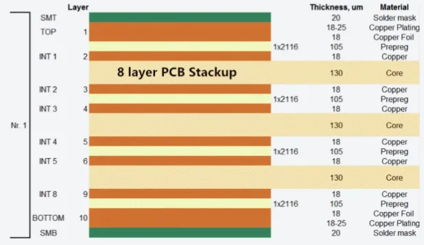
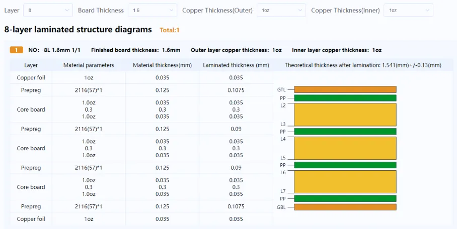
Layer Stackup Optimization
The precise arrangement of the eight layers in the stackup is a foundational design step. This involves designating layers for signals, ground planes, and power planes in an order that optimizes electrical performance and minimizes electromagnetic interference. AIVON can provide tailored recommendations for stackup structures based on specific parameters such as total board thickness, inner copper thickness, and outer copper thickness, offering detailed laminated structure diagrams for guidance.
Suggested Reading: From Schematic to Reality: A Practical Guide to 8-Layer PCB Layout
Strategic Routing Directions
To minimize crosstalk between adjacent signal layers, it is a best practice to route these layers perpendicularly to one another. This orthogonal routing strategy significantly helps in preserving signal integrity, which is especially vital in circuits operating at high speeds and frequencies.
Return Path Management
High-speed signals critically depend on a clear, direct, and short return path to ground to avoid interference and maintain signal quality. Designers must ensure that these return paths do not overlap or intersect with other signal traces, which could compromise signal integrity and introduce noise.
Ground Plane Integrity
A continuous and unbroken ground plane is fundamental for reducing impedance discontinuities and establishing a stable reference voltage for all signal layers. Splitting the ground plane can introduce severe performance issues, making it imperative to maintain its integrity across the board design.
How Are 8-Layer PCBs Manufactured?
The fabrication of 8-layer PCBs is a complex process demanding high precision and specialized materials to achieve the desired performance and reliability.
Material Selection Considerations
The choice of materials for each layer profoundly impacts the final performance of an 8-layer PCB. While standard FR-4 material is commonly used for core and prepreg layers in general applications, high-speed or high-frequency designs may necessitate advanced materials like Rogers, Isola, or Arlon.
● FR-4 (Standard): Characterized by low cost and good mechanical strength, typically used in consumer electronics.
● High-Tg FR-4: Offers enhanced temperature resistance, suitable for automotive and industrial applications.
● Polyimide: Provides excellent thermal stability, often found in aerospace and military hardware.
● Rogers/Isola/Arlon: Features low dielectric loss, ideal for RF, 5G, and radar systems requiring superior high-frequency signal performance.
Precision Layer Alignment and Bonding
During manufacturing, the accurate alignment of all eight layers is absolutely critical for the PCB's functionality. These layers are then fused together under carefully controlled heat and pressure, forming a robust and unified multi-layer structure.
Etching, Drilling, and Plating Processes
The conductive layers undergo precise etching to create the intricate circuit patterns. Subsequently, holes are drilled through the stackup, and these holes are then plated with copper to form vias, which electrically connect different layers. These processes require extremely high precision to preserve the integrity of the design.
Rigorous Quality Control and Testing
Throughout the manufacturing cycle, stringent quality control measures are implemented to ensure the reliability of 8-layer PCBs. This includes detailed visual inspections, comprehensive electrical testing, and thermal analysis to identify any potential defects or performance deviations.
What Are the Common Applications for 8-Layer PCBs?
8-layer PCBs are indispensable across a wide array of advanced electronic applications due to their capacity for complex circuitry, enhanced signal integrity, and efficient power management.
Key Industry Sectors
● Telecommunications: Utilized in communication equipment for managing intricate signal routing and robust power distribution, guaranteeing reliable network performance.
● Aerospace and Defense: Essential in demanding aerospace and defense systems that require high-performance, robust, and dependable circuit boards capable of extreme complexity.
● Power Electronics: Found in critical applications such as electric vehicle control systems, industrial power inverters, and high-efficiency power supplies. These PCBs are designed to handle high current loads while maintaining optimal thermal performance, facilitated by dedicated power and ground planes for efficient current return.
● Automotive Industry: Integral to modern vehicle electronic systems, controlling everything from advanced driver-assistance systems (ADAS) to infotainment. 8-layer PCBs manage the inherent complexity of these automotive electronic circuits.
● Internet of Things (IoT) Devices: Critical for IoT hardware like smart sensors, wearable tech, and home automation controllers. These devices demand compact, energy-efficient designs that can seamlessly integrate wireless protocols (Wi-Fi, Bluetooth, Zigbee). The additional layers allow for complex routing in tight spaces and minimize crosstalk.
Combining Rigidity and Flexibility: 8-Layer Flex-Rigid PCBs
Designers often integrate both rigid and flexible layers within 8-layer PCBs to achieve a hybrid structure known as rigid flex PCBs. This approach offers a unique blend of durability and flexibility, making them ideal for specialized applications.
Advantages of Flex-Rigid Designs
● Reduced Size and Weight: Flex-rigid boards can conform to irregular shapes, allowing for more compact and lighter electronic assemblies.
● Enhanced Durability: They offer improved resistance to vibration and mechanical movement compared to purely rigid boards.
● Dynamic Routing: Provides flexibility for routing in extremely tight or constrained spaces, such as in foldable devices, advanced cameras, and aerospace systems.
Essential Guidelines for Safe Handling and Assembly
Working with multilayer PCBs, especially complex 8-layer boards, requires adherence to specific safety and best practice guidelines during assembly, soldering, and ongoing maintenance.
Best Practices for Handling
● ESD Protection: Always utilize Electrostatic Discharge (ESD) protective measures, such as wrist straps and mats, to prevent static electricity from damaging sensitive components.
● Mechanical Stress Avoidance: Handle the boards carefully to avoid applying excessive mechanical stress to connectors, vias, and other delicate components.
● Controlled Soldering: For multilayer boards, preheating the entire assembly before soldering is recommended. This helps to prevent thermal shock and reduce the risk of board warping or delamination.
What Does the Future Hold for 8-Layer PCBs?
The demand for 8-layer PCBs is steadily rising, driven by the rapid evolution of advanced technologies like AI chips, autonomous driving systems, quantum computing, and 5G infrastructure. Innovation continues to push the boundaries of what these multi-layer boards can achieve.
Emerging Trends and Innovations
● Ultra-Thin Dielectric Materials: Development of thinner insulating layers will enable higher signal speeds and even more compact designs.
● Embedded Passive Components: Integrating resistors, capacitors, and inductors directly into the PCB layers will further reduce board size and enhance performance.
● AI-Integrated Design Tools: Advanced simulation tools, integrated with artificial intelligence, will optimize complex high-speed designs more efficiently.
● Improved Thermal Via Management: Innovations in thermal via design and placement will enhance heat dissipation for increasingly power-dense systems.
Conclusion: Mastering 8-Layer PCB Technology
The 8-layer PCB stands as a testament to the cutting edge of PCB design and manufacturing. Its inherent capability to support complex circuits, significantly improve signal integrity, and efficiently manage power distribution makes it an essential component in the most advanced electronic devices of today and tomorrow. Whether you are an electronic engineer, a dedicated PCB designer, or a burgeoning tech startup, acquiring a deep understanding of 8-layer PCBs can profoundly elevate your project capabilities.
For specialized support and expert guidance, consider connecting with AIVON. We offer comprehensive resources to explore advanced PCB design and manufacturing best practices. The future of electronics is undeniably multi-layered, and a mastery of 8-layer PCBs is your key to remaining at the forefront of this dynamic and rapidly evolving field.


