What is a 4-Layer PCB Stackup and Why is it Critical?
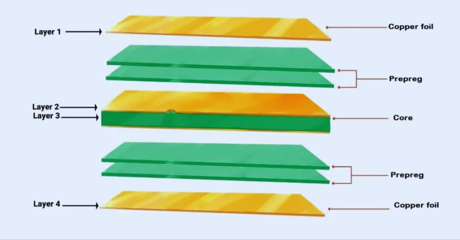
A 4-layer PCB stackup defines the precise arrangement of conductive copper layers and insulating dielectric materials within a printed circuit board that features four copper layers. In contrast to simpler 2-layer designs, a 4-layer configuration provides expanded real estate for routing signals and dedicated planes for power and ground, making it an ideal choice for compact, high-speed, or noise-sensitive electronic applications. The stackup dictates the order of these layers, typically positioning signal layers on the exterior surfaces and placing power and ground planes in the interior.
The importance of optimizing a PCB stackup cannot be overstated. An inadequately designed stackup can lead to a host of problems, including electromagnetic interference (EMI), signal crosstalk, and impedance mismatches. For example, incorrect spacing between layers can introduce signal delays or unwanted noise coupling, which directly impacts overall circuit performance. By meticulously planning your 4-layer PCB design, you can significantly mitigate these risks, bolster signal integrity, and ensure stable operation, even for digital circuits functioning at frequencies exceeding 100 MHz.
Which 4-Layer PCB Stackup Configurations Are Most Common?
When developing a four layer PCB, the specific arrangement of layers significantly influences the board's electrical performance. Here are the most frequently utilized stackup configurations in 4 layer PCB design, highlighting their advantages and typical applications.
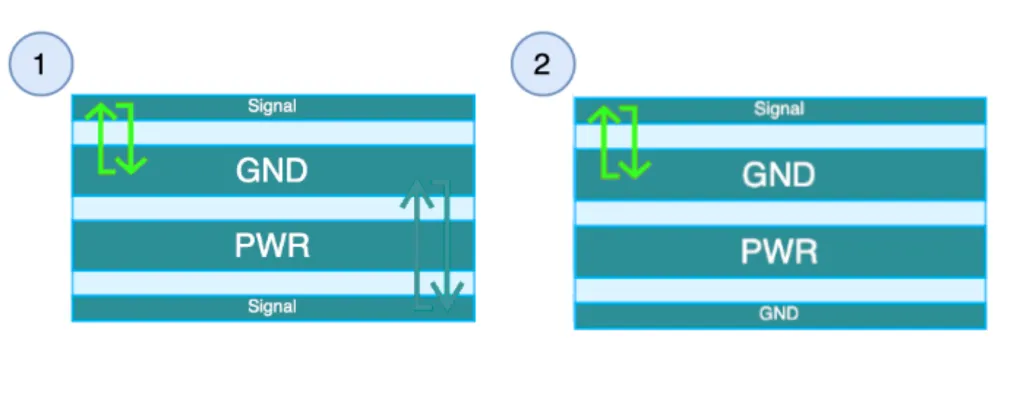
Signal-Ground-Power-Signal (SGPS) Stackup
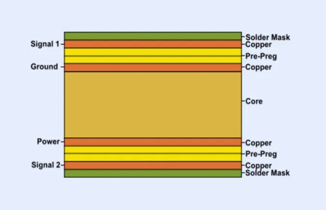
This configuration represents the most widely adopted 4-layer PCB stackup. In an SGPS arrangement, the uppermost (Layer 1) and lowermost (Layer 4) layers are designated for signal routing. The internal layers are assigned as a solid ground plane (Layer 2) and a power plane (Layer 3). Placing the ground plane directly beneath the top signal layer provides an excellent low-impedance return path for signals and helps significantly in reducing EMI, thereby aiding in regulatory compliance.
● Advantages: Offers superior signal integrity due to the close proximity of signal layers to a solid ground plane; provides effective shielding against noise.
● Typical Use Case: Ideal for high-speed digital circuits, such as designs incorporating microcontrollers or FPGAs operating at frequencies above 50 MHz.
● Design Insight: To maintain tight coupling and precise impedance control—often targeting 50 ohms for high-speed traces—it's advisable to keep the dielectric thickness between the top signal layer and the ground plane minimal (e.g., around 0.2 mm).
Signal-Power-Ground-Signal (SPGS) Stackup
This alternative configuration places the power plane on Layer 2 and the ground plane on Layer 3. While less conventional than SGPS, this setup can be advantageous when power delivery needs to be optimized for specific components located predominantly on the top layer.
● Advantages: Provides enhanced power distribution, particularly beneficial for components situated on the top signal layer.
● Typical Use Case: Suited for designs with substantial power demands on the top layer, such as power amplifier circuits.
● Design Insight: Despite the power plane's placement, ensure the ground plane on Layer 3 remains robust enough to provide a stable return path for signals on the bottom layer to prevent noise-related issues.
Suggested Reading: Designing with Four-Layer PCBs: A Comprehensive Guide
What Are the Key Design Factors for 4-Layer PCBs?
Optimizing a PCB layer stackup involves more than simply selecting a layer configuration. Several critical factors must be considered during the design phase to ensure both high performance and manufacturability.
Layer Thickness and Dielectric Material Choices
The thickness of the insulating dielectric material separating conductive layers directly impacts signal impedance and propagation speed. For high-speed designs, a thinner dielectric (e.g., 0.1 to 0.2 mm) between signal and ground layers is crucial for maintaining controlled impedance, often aiming for 50 or 75 ohms for differential pairs. Standard FR-4 material, with a dielectric constant (Dk) typically between 4.2 and 4.5, is widely used. However, for applications involving frequencies above 1 GHz, low-loss materials like Rogers, which have a Dk of 3.0 to 3.5, should be considered to minimize signal attenuation.
● Practical Tip: Utilize a stackup calculator tool to precisely determine the required dielectric thickness to achieve your target impedance. For example, to achieve a 50-ohm trace on a 1.6 mm thick FR-4 PCB, a trace width of approximately 0.3 mm with a 0.2 mm dielectric spacing to the ground plane might be necessary.
Power and Ground Plane Integrity
The inclusion of dedicated power and ground planes is a significant advantage of a 4-layer PCB stackup. A continuous, solid ground plane is fundamental for reducing noise by providing a stable, low-impedance return path for all signals. It is crucial to avoid splitting the ground plane unless absolutely unavoidable, as splits can create undesirable current loops and increase electromagnetic interference. Similarly, ensure the power plane is also continuous and positioned in close proximity to the ground plane. This arrangement effectively forms a distributed capacitance, which helps in reducing power supply noise.
● Practical Tip: Position decoupling capacitors (e.g., 0.1 μF) as close as possible to the power pins of integrated circuits. Connect them directly to the power and ground planes using very short vias to efficiently filter out high-frequency noise.
Signal Routing and Trace Placement Strategies
In a 4-layer PCB design, signal traces are typically routed on the outer layers (top and bottom). High-speed signals should ideally be routed on the layer most proximate to the solid ground plane (usually the top layer in an SGPS stackup) to minimize interference and ensure a clear return path. Keeping critical signal trace lengths as short as possible helps to reduce signal propagation delays; signals travel at approximately 150 mm/ns on FR-4 material, meaning a 150 mm trace introduces a 1 ns delay.
● Practical Tip: For differential pairs, it is essential to maintain consistent spacing (e.g., 0.2 mm) between the traces and ensure accurate length matching, typically within 0.5 mm, to prevent signal skew in high-speed protocols like USB or HDMI.
Related Reading: Differential vs Single-Ended Outputs
How Can a 4-Layer PCB Stackup Be Further Optimized?
Beyond the fundamental design principles, several advanced strategies can fine-tune your PCB stackup for peak performance and long-term reliability. These approaches address common challenges encountered in 4-layer PCB design.
Reducing Crosstalk through Layer Spacing
Crosstalk, the unwanted coupling between adjacent signal traces or layers, can severely degrade signal quality. In a 4-layer PCB, crosstalk can occur between the top and bottom signal layers if they are positioned too closely. To mitigate this, increase the dielectric thickness between these signal layers (e.g., to 0.8 mm or more), while simultaneously maintaining tight signal-to-ground spacing (e.g., 0.2 mm). This approach effectively reduces coupling between distinct signal layers while preserving excellent impedance control for individual traces.
Related Reading: Routing Challenges and Solutions on 4-Layer PCBs
Strategic Use of Vias
Vias are essential for connecting traces between different layers, but their improper use can introduce unwanted inductance and signal reflections. For high-speed signals, opt for microvias or blind vias to minimize stub length, which is a common source of reflections. Always place ground vias in close proximity to signal vias to ensure a continuous and low-inductance return path. For critical signals, limit via transitions to one or two per net to prevent excessive signal delays and impedance discontinuities.
Effective Thermal Management Planning
In designs that incorporate high-power components, effective heat dissipation becomes a critical concern. Utilize the robust power and ground planes to help spread heat by connecting thermal vias from hot components directly to these planes. For example, a power IC dissipating 2W might necessitate 4 to 6 thermal vias, each with a diameter of 0.3 mm, to efficiently transfer heat away from the component.
Simulation and Rigorous Testing
Before committing to the final 4-layer PCB stackup, it is highly recommended to employ simulation tools to model signal integrity and impedance characteristics. These tools can predict potential issues like ringing or overshoot in high-speed signals, allowing for crucial adjustments to layer spacing or trace widths. Following PCB manufacturing, thoroughly test the physical board using an oscilloscope to verify signal quality; look for clean signal edges with rise times typically under 1 ns for high-speed signals.
What Are Common Mistakes to Avoid in 4-Layer PCB Stackup Design?
Even experienced designers can encounter pitfalls during PCB layer stackup planning. Being aware of these common errors can help you avoid them:
● Splitting Ground Planes: Fragmenting the ground plane for routing convenience can inadvertently create noise-generating loops and compromise signal integrity. Always prioritize a continuous and unbroken ground plane.
● Ignoring Impedance Control: Failing to precisely calculate trace widths and layer spacing for controlled impedance can severely degrade signal quality, particularly at frequencies exceeding 100 MHz.
● Overloading Signal Layers: Routing an excessive number of traces on a single layer can lead to signal congestion, increased crosstalk, and routing difficulties. Distribute signals as evenly as possible between the top and bottom signal layers.
● Poor Via Placement: Placing vias far from their corresponding ground planes can interrupt the critical return paths for high-frequency currents, leading to increased noise and EMI. Ensure vias are always placed in close proximity to their reference planes.
Diverse Applications Benefiting from 4-Layer PCB Stackups
A meticulously designed 4-layer PCB stackup is incredibly versatile and well-suited for a broad spectrum of applications across various industries.
● Consumer Electronics: Devices like smartphones and tablets leverage 4-layer PCBs to integrate high-speed digital signals and complex power distribution networks within remarkably compact form factors.
● Industrial Control Systems: Programmable Logic Controllers (PLCs) and advanced automation systems benefit greatly from the enhanced noise immunity provided by dedicated ground planes in a 4-layer design, ensuring reliable operation in demanding industrial environments.
● Automotive Systems: Critical components such as Engine Control Units (ECUs) and various sensor modules rely on robust 4-layer designs to ensure high reliability and performance, even when subjected to harsh automotive operating conditions.
Conclusion: The Foundation for Superior 4-Layer PCB Performance
Optimizing a 4-layer PCB stackup is a delicate balance that integrates considerations for signal integrity, effective noise reduction, and manufacturability. By making informed choices regarding layer configuration, such as the widely favored Signal-Ground-Power-Signal (SGPS) arrangement, and diligently addressing factors like layer spacing, strategic via placement, and precise impedance control, you can engineer a design that delivers consistent reliability even in the most demanding applications. It is crucial to remember the importance of simulating your design, thoroughly testing prototypes, and actively avoiding common pitfalls such as splitting ground planes or neglecting thermal management requirements.
Whether your project involves high-speed digital circuits or power-intensive systems, a carefully planned PCB layer stackup serves as the bedrock of success. Leverage the insights and actionable strategies provided in this guide to streamline your 4-layer PCB design process, ultimately achieving superior results for your next electronic innovation.


